
Large-area single-layer semiconductor two-dimensional WS2 film material and preparation method and application thereof

A thin-film material, large-area technology, applied in the field of materials, can solve problems such as unfavorable commercial applications, increase experimental costs, pollution, etc., and achieve excellent light response speed, low cost, and good controllability.

Pending Publication Date: 2021-12-07
XIDIAN UNIV
View PDF4 Cites 0 Cited by
  • Summary
  • Abstract
  • Description
  • Claims
  • Application Information

AI Technical Summary

Problems solved by technology

Jiadong Zhou et al. used the method of adding NaCl to form the gaseous compound WO 2 Cl 2 , thereby significantly reducing the WO 3 The melting point of , but this method due to the addition of additional substances, so the resulting WS 2 The sample produced certain pollution (Nature, 2018, 556, 355-359.); Wencai Ren et al. used the strong interaction between gold foil and S to synthesize a large-area monolayer WS on a gold foil substrate. 2 materials, but the use of gold foil greatly increases the cost of experiments, which is not conducive to WS 2 Subsequent commercial application (Nat.Commun., 2015,6,8569.)

Method used


Image

  • Large-area single-layer semiconductor two-dimensional WS2 film material and preparation method and application thereof
  • Large-area single-layer semiconductor two-dimensional WS2 film material and preparation method and application thereof
  • Large-area single-layer semiconductor two-dimensional WS2 film material and preparation method and application thereof

Examples


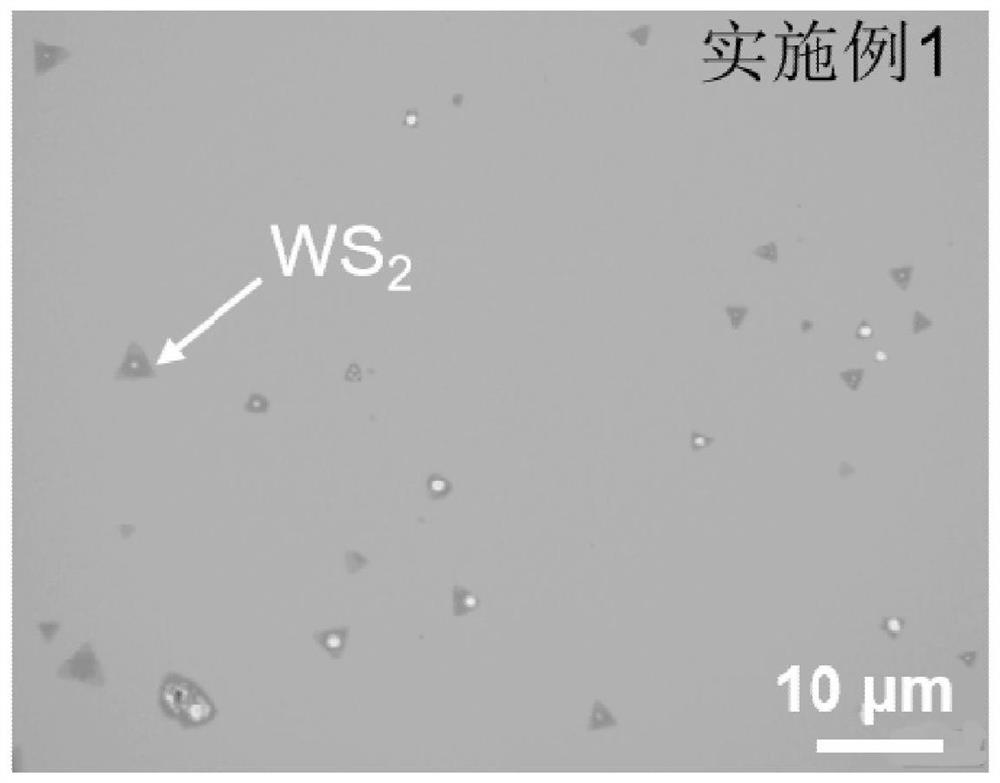
Embodiment 1

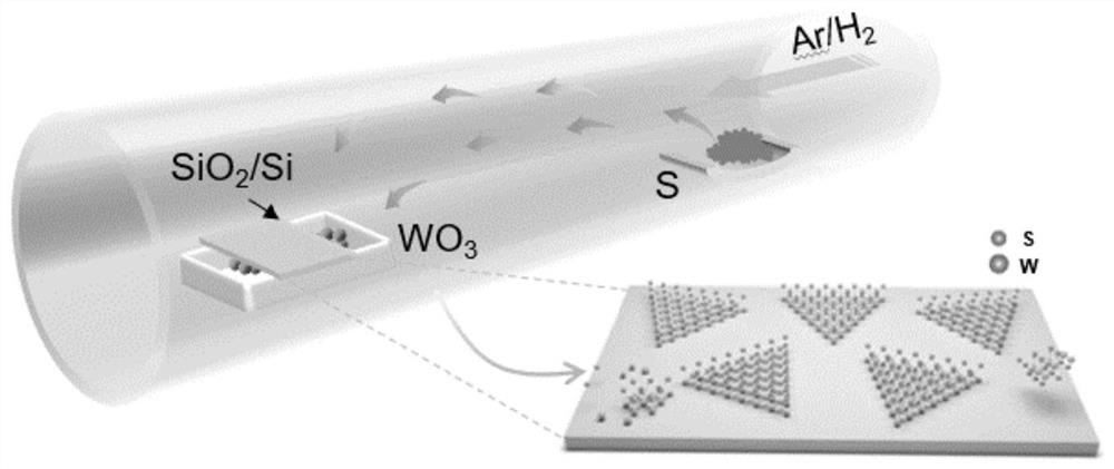
[0034] Preparation of large-area monolayer semiconductor two-dimensional WS 2 A method for thin film materials, comprising the steps of:

[0035] 1) Weigh 50mg WO 3 Placed in a ceramic boat in the center of a tube furnace in a quartz tube; place two silicon wafers with a thickness of 1*1cm and a silicon dioxide layer of 300nm upside down on the WO 3 On the ceramic boat; Take by weighing 100mg sulfur powder and place in the ceramic boat and be positioned at the position of 15cm away from the center of the upstream of the quartz tube;

[0036] 2) Pass into the argon gas of 300sccm in the tube furnace, the aeration time is 10min, to get rid of the air in the tube, after 10min, the argon flow rate is adjusted to 100sccm;

[0037] 3) Start heating, and after reaching the set growth temperature of 850°C, grow under this condition for 10 minutes; at this moment, the temperature corresponding to the sulfur powder is 200°C.

[0038] Stop heating, cool down to room temperature natura...

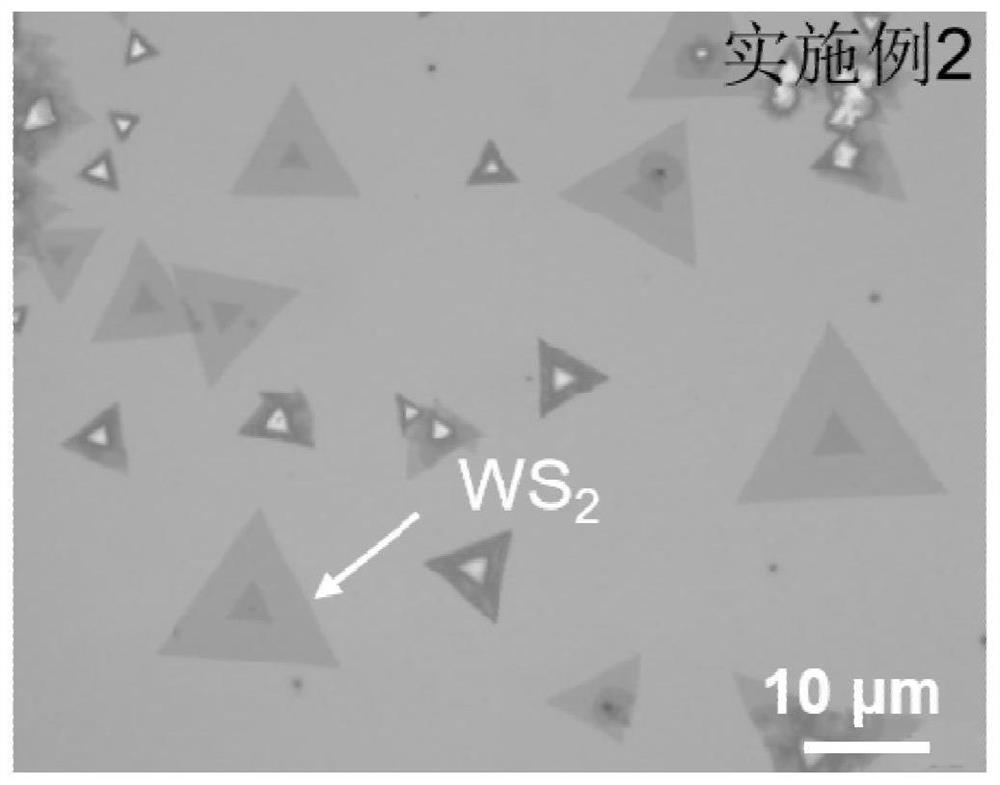
Embodiment 2

[0040] The difference from Example 1 is that step 3) is: first open the hydrogen valve, set the hydrogen flow rate to 20 sccm and start heating, and after reaching the set growth temperature of 850 ° C, grow under this condition for 10 min; at this moment, the sulfur powder corresponds to The temperature is 200° C., and other condition parameters are the same as in Example 1.

Embodiment 3

[0042] The difference from Example 1 is that step 3) is: start heating, and after reaching the set growth temperature of 850°C, open the hydrogen valve, set the hydrogen flow rate to 20 sccm, and grow for 10 minutes under this condition; at this moment, the temperature corresponding to the sulfur powder is 200°C, other condition parameters are the same as in Example 1.

[0043] For the large-area single-layer semiconductor two-dimensional WS prepared in the above examples 2 Morphological and structural characterization of thin film materials:

[0044] 1. Reference figure 2 , image 3 and Figure 4 Respectively, WS grown without feeding hydrogen, continuously feeding hydrogen and feeding hydrogen after reaching the preset temperature during the growth process 2 Comparison of the optical microscope photos, the microscope model is BX51 produced by Olympus Corporation. It can be seen from the figure that when no hydrogen is introduced, the samples are scattered on the silica...


PUM

PropertyMeasurementUnit
Horizontal sizeaaaaaaaaaa

Abstract

The invention discloses a large-area single-layer semiconductor two-dimensional WS2 film material and a preparation method and application thereof, and belongs to the technical field of materials. WO3 and S are taken as precursors, argon is taken as carrier gas, nucleation and growth of WS2 can be effectively controlled by adjusting the introduction opportunity of hydrogen, and preparation of large-area and layer-number-controllable WS2 is realized. The method provided by the invention is low in cost, good in controllability and strong in repeatability. The large-area single-layer semiconductor two-dimensional WS2 film material prepared by the method has the characteristics of a large area, a single crystal type and the like, so that the large-area single-layer semiconductor two-dimensional WS2 film material can show excellent light response speed in a photoelectric detector device and has practical value.

Description

technical field [0001] The invention belongs to the field of material technology, in particular to a semiconductor two-dimensional WS 2 The preparation method of thin film materials can be used to make field effect transistors and photodetectors. Background technique [0002] WS 2 It is a two-dimensional layered semiconductor material that exhibits high fluorescence quantum yield at room temperature, and also has obvious spin-orbit coupling. These excellent properties make it widely used in the field of electronic and optoelectronic devices prospect. Whether it can be applied in the end depends on the large-area single-layer WS 2 Whether controllable equipment can be realized. Currently, two-dimensional WS 2 The preparation methods of materials mainly include mechanical exfoliation, liquid phase exfoliation, and chemical vapor deposition. Compared with the first two methods, chemical vapor deposition has become the most widely used method because of its high growth effi...

Claims


Application Information

Patent Timeline
IPC IPC(8): C23C16/30C30B25/02C30B29/46G01D5/26
CPCC23C16/305C30B25/02C30B29/46G01D5/26
Inventor 杨如森李晓波张建斌周楠
Owner XIDIAN UNIV
Learn More