


Quick Research
Generate reliable direction feasibility study reports for your R&D in just a few steps.

Technical Q&A
Discover and master advanced knowledge NOW. Basics, ideas, possibilities, all at once.

Find Solutions
As an expert in R&D theories, this can generate solutions to your technical problems instantly.

Evaluate Feasibility
Analyze your overall solution with one click, know your potential R&D risks in advance.

Monitor Landscape
Get weekly tech updates, stay abreast of the latest tech innovations and key insights.
Si-based GaN epitaxial low-dislocation film and preparation method thereof
A low-dislocation and epitaxy technology, applied in the field of microelectronics, which can solve problems such as cracks, stacking faults, and thin-film dislocations
- Summary
- Abstract
- Description
- Claims
- Application Information
AI Technical Summary
Problems solved by technology
Method used
Image


Examples
Embodiment 1
[0027] Growth in MOCVD system by metal organic chemical vapor deposition:
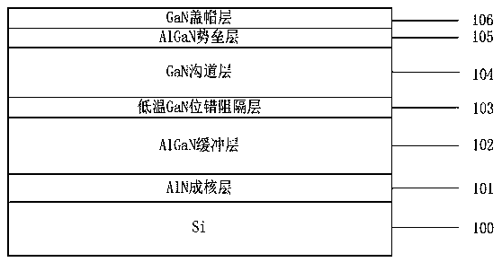
[0028] 1. First put the Si substrate into the reaction chamber and raise the temperature to 1100°C, and remove the oxide film on the surface under H2 conditions;
[0029] 2. On the basis of the above steps, the temperature is lowered to 1000° C., and a layer of ALN nucleation layer is grown with a thickness of 100 nm. The film thickness is realized by controlling the deposition time and cooperating with MOCVD monitoring system.
[0030] 3. Based on the above steps, the temperature is raised to 1100° C., and an ALGaN buffer layer is grown with a thickness of 1 μm.
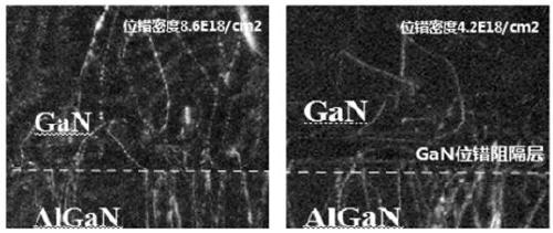
[0031] 4. On the basis of the previous steps, the temperature was lowered to 800° C., and a dislocation barrier layer with a thickness of 200 nm was grown.
[0032] 5. On the basis of the above steps, the temperature is raised to 1100° C., and the GaN channel layer, AlGaN barrier layer and GaN cap layer are grown, with thicknesses of 2um, ...
Embodiment 2
[0034] Growth in MOCVD system by metal organic chemical vapor deposition:
[0035] 1. First put the Si substrate into the reaction chamber and raise the temperature to 1100°C, and remove the oxide film on the surface under H2 conditions;
[0036] 2. On the basis of the above steps, the temperature is lowered to 1000° C., and a layer of ALN nucleation layer is grown with a thickness of 100 nm. The film thickness is realized by controlling the deposition time and cooperating with MOCVD monitoring system.
[0037] 3. Based on the above steps, the temperature is raised to 1100° C., and an ALGaN buffer layer is grown with a thickness of 1 μm.
[0038] 4. On the basis of the above steps, the temperature is lowered to 800° C., and a dislocation barrier layer with a thickness of 300 nm is grown.
[0039] 5. On the basis of the above steps, the temperature is raised to 1100° C., and the GaN channel layer, AlGaN barrier layer and GaN cap layer are grown, with thicknesses of 2um, 30nm,...
Embodiment 3
[0041] Growth in MOCVD system by metal organic chemical vapor deposition:
[0042] 1. First put the Si substrate into the reaction chamber and raise the temperature to 1100°C, and remove the oxide film on the surface under H2 conditions;
[0043] 2. On the basis of the above steps, the temperature is lowered to 1000° C., and a layer of ALN nucleation layer is grown with a thickness of 100 nm. The film thickness is realized by controlling the deposition time and cooperating with MOCVD monitoring system.
[0044] 3. Based on the above steps, the temperature is raised to 1100° C., and an ALGaN buffer layer is grown with a thickness of 1 μm.
[0045] 4. On the basis of the above steps, the temperature is lowered to 800° C., and a dislocation barrier layer with a thickness of 400 nm is grown.
[0046] 5. On the basis of the above steps, the temperature is raised to 1100° C., and the GaN channel layer, AlGaN barrier layer and GaN cap layer are grown, with thicknesses of 2um, 30nm,...
PUM
| Property | Measurement | Unit |
|---|---|---|
| thickness | aaaaa | aaaaa |
| thickness | aaaaa | aaaaa |
| thickness | aaaaa | aaaaa |
Abstract
Description
Claims
Application Information
 - R&D Engineer
- R&D Manager
- IP Professional
- Industry Leading Data Capabilities
- Powerful AI technology
- Patent DNA Extraction
Browse by: Latest US Patents, China's latest patents, Technical Efficacy Thesaurus, Application Domain, Technology Topic, Popular Technical Reports.
© 2024 PatSnap. All rights reserved.Legal|Privacy policy|Modern Slavery Act Transparency Statement|Sitemap|About US| Contact US: help@patsnap.com