


Quick Research
Generate reliable direction feasibility study reports for your R&D in just a few steps.

Technical Q&A
Discover and master advanced knowledge NOW. Basics, ideas, possibilities, all at once.

Find Solutions
As an expert in R&D theories, this can generate solutions to your technical problems instantly.

Evaluate Feasibility
Analyze your overall solution with one click, know your potential R&D risks in advance.

Monitor Landscape
Get weekly tech updates, stay abreast of the latest tech innovations and key insights.
Thyristor chip junction terminal structure
A thyristor and junction terminal technology, applied in the field of semiconductor power devices, can solve the problems of poor thermal conductivity in the P1 area of the anode, short circuit of the device, and occupation of the effective area of the cathode, so as not to be easily damaged by chipping, increase the effective area, and reduce manufacturing costs Effect
- Summary
- Abstract
- Description
- Claims
- Application Information
AI Technical Summary
Problems solved by technology
Method used
Image

Examples
Embodiment 2
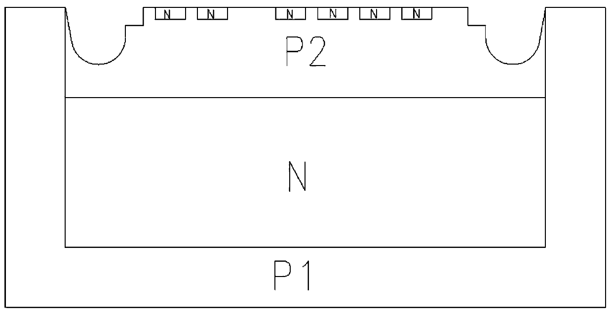
[0033] Embodiment 2: as Figures 10 to 12 As shown, a thyristor chip junction terminal structure includes a long base region N, an anode region P1, a short base region P2, and a cathode region N arranged on the short base region P2 + , the short-circuit point 6 and the gate control area 7, a P-type protrusion 3 formed by diffusion is partially provided on the long base area N, and the P-type protrusion 3 communicates with the anode area P1 as a whole. The short base region P2 is extended downward with a voltage groove 1, the P-type boss 3 is located below the voltage groove 1, and the bottom of the voltage groove 1 is on the P-type boss 3 or partially on the long base region N , partly located on the P-shaped boss. The P-type mesa 3 includes a P-type region 301 adjacent to the long base region N and a P+-type buffer barrier layer 302 outside the P-type region 301 . The P-type region 301 and the P+-type buffer barrier layer 302 are formed by diffusion of P-type impurities. In...
Embodiment 3
[0035] Embodiment 3: As another formation structure of the P-type region 301 and the P+-type buffer barrier layer 302, the side edge of the anode region P1 is provided with a circle of step grooves 13 with at least one step, preferably, a step groove 13 is provided with a two-level stepped structure, such as Figure 13 As shown, the step groove 13 includes a first step 131 and a second step 132, the depth h1 of the first step 131 is 50-80um, the depth h2 of the second step 132 is 30-50um, and the width L1 of the first step 131 is 100 ~200um, the width L2 of the second step 132 is 50~100um. In actual production, two adjacent chips share a groove, the grooves are designed symmetrically, and formed as follows after dicing: Figure 12 The single-side stepped groove 13 structure shown. After the P-type impurity is diffused in the stepped groove 13, a stepped P-type boss is formed on the long base region N. At the same height, the concentration of the P-type impurity above the fir...
Embodiment 4
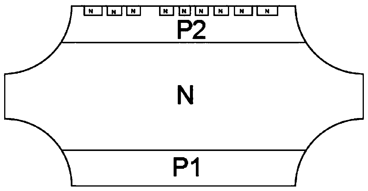
[0036] Embodiment 4: Taking a chip with a withstand voltage of 2000V and a current of 100A as an example, the chip pattern design is 17mmx17mm, the total thickness is 420um, the thickness of the anode region P1 is 90um, and the short base region P2 is 90um.
[0037] Using a thyristor chip with a P-type isolation wall bilateral voltage groove structure, such as figure 2 In the shown structure, the width of the separation wall is 0.3mm, the width of the voltage groove is 0.9mm, and the voltage groove on both sides is a voltage groove with a stepped structure, therefore, the width of the cathode region is 17-(0.3+0.9)x2= 14.6mm, the area of the cathode area is 14.6mmx14.6mm=213mm 2 .
[0038] Using the thyristor chip with the P-type boss structure described in Embodiment 1, the depth of the blind hole is preferably 80um, so that the P-type boss 3 is about 80um higher than the anode region P1, and the P-type boss 3 is a lower concentration. P-type impurity composition. The P...
PUM
| Property | Measurement | Unit |
|---|---|---|
| Overall width | aaaaa | aaaaa |
| Width | aaaaa | aaaaa |
Abstract
Description
Claims
Application Information
 - R&D Engineer
- R&D Manager
- IP Professional
- Industry Leading Data Capabilities
- Powerful AI technology
- Patent DNA Extraction
Browse by: Latest US Patents, China's latest patents, Technical Efficacy Thesaurus, Application Domain, Technology Topic, Popular Technical Reports.
© 2024 PatSnap. All rights reserved.Legal|Privacy policy|Modern Slavery Act Transparency Statement|Sitemap|About US| Contact US: help@patsnap.com