A resistive variable layer self-selection resistive variable memory and its construction method and application
A technology of resistive variable memory and construction method, which is applied in the direction of electrical components, etc., to achieve the effects of good thermal stability, good industrial compatibility, and easy process control
- Summary
- Abstract
- Description
- Claims
- Application Information
AI Technical Summary
Problems solved by technology
Method used
Image
Examples
Embodiment 1
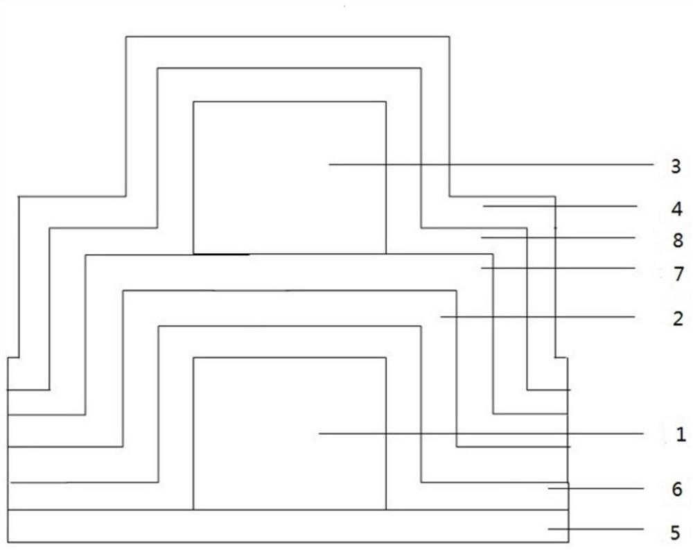
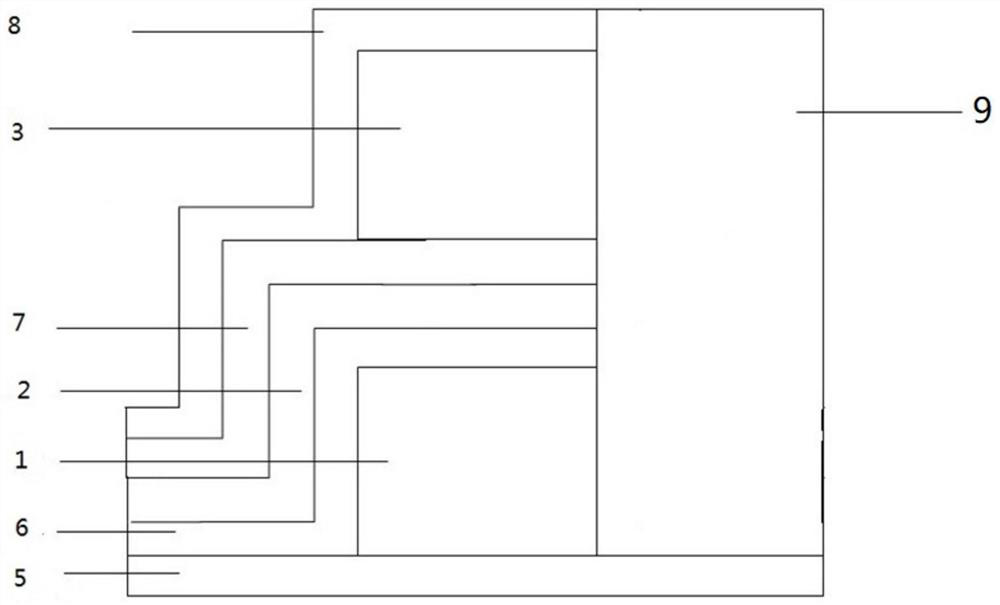
[0063] A resistive variable layer self-selection resistive variable memory, comprising a stacked layer; the stacked layer includes a fourth Hf layer 4, a fourth Si 3 N 4 Layer 8, third Hf layer 3, third Si 3 N 4 Layer 7, second Hf layer 2, second Si 3 N 4 Layer 6, first Hf layer 1 and first Si 3 N 4 Layer 5; the left and right sides of the stacked layer are respectively provided with a bottom electrode and a top electrode; the bottom electrode and the fourth Si 3 N 4 Layer 8, the third Si 3 N 4 Layer 7 communicates with the second Hf layer 2 and is arranged on the upper surface of the second Hf layer 2; the top electrode communicates with the entire stack layer and is arranged on the first Si 3 N 4 top surface of layer 5.
[0064] First Si 3 N 4 The thickness of layer 5 is 25nm; the thickness of the first Hf layer 1 is 110nm; the second Si 3 N 4 The thickness of layer 6 and the second Hf layer 2 is 25nm; the third Si 3 N 4 The thickness of layer 7 is 25nm; the...
Embodiment 2
[0067] The resistive variable layer self-selectable resistive variable memory as described in Embodiment 1, the difference is that the resistive variable layer self-selectable resistive variable memory comprises two stacked layers arranged side by side; the top electrode is a bit line; the for the word line.
Embodiment 3
[0069] A method for constructing a resistive variable layer self-selecting resistive variable memory as described in Embodiment 1, comprising the following steps:
[0070] 1) Deposit the first Si on the substrate 3 N 4 Layer 5; depositing the first Si on the substrate 3 N 4 Layer 5 is realized by CVD method; the substrate is a Si substrate;
[0071] 2) In the first Si 3 N 4 Deposit the first Hf layer 1 on the layer 5, then perform photolithography and lift-off treatment; 3 N 4 The deposition of the first Hf layer 1 on the layer 5 is achieved by a DC sputtering method.
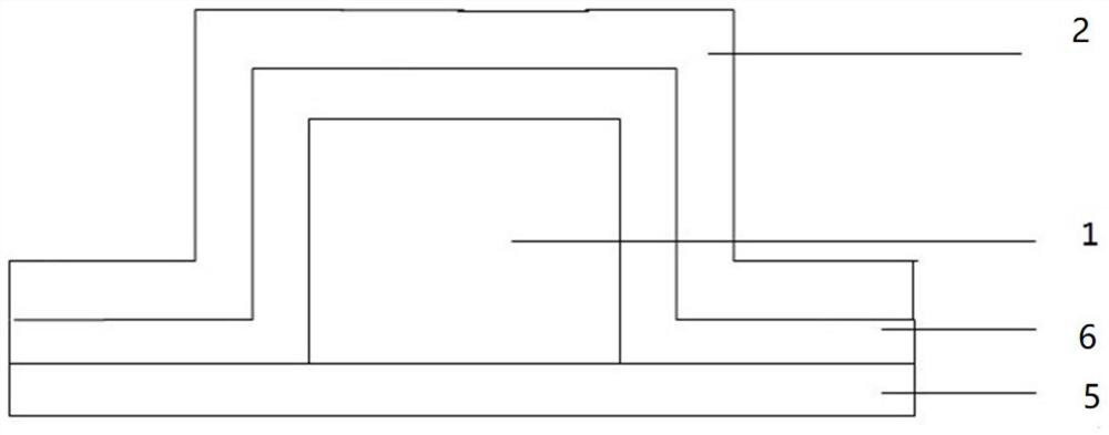
[0072] 3) Deposit the second Si sequentially on the first Hf layer 1 3 N 4 Layer 6, the second Hf layer 2; as figure 1 shown. Second Si 3 N 4 Layer 6 is deposited by CVD method and the second Hf layer 2 is deposited by sputtering.
[0073] 4) Deposit the third Si on the second Hf layer 2 3 N4 Layer 7, according to the method of step 2), 3) in the third Si 3 N 4 Deposit the third Hf layer 3, the...
PUM
| Property | Measurement | Unit |
|---|---|---|
| thickness | aaaaa | aaaaa |
| thickness | aaaaa | aaaaa |
| thickness | aaaaa | aaaaa |
Abstract
Description
Claims
Application Information
 - R&D Engineer
- R&D Manager
- IP Professional
- Industry Leading Data Capabilities
- Powerful AI technology
- Patent DNA Extraction
Browse by: Latest US Patents, China's latest patents, Technical Efficacy Thesaurus, Application Domain, Technology Topic, Popular Technical Reports.
© 2024 PatSnap. All rights reserved.Legal|Privacy policy|Modern Slavery Act Transparency Statement|Sitemap|About US| Contact US: help@patsnap.com


