Millimeter-wave and terahertz-wave direct modulator and fabrication method thereof

A modulator, a direct technology, applied in the direction of semiconductor devices, semiconductor/solid-state device manufacturing, electrical components, etc., can solve the problems of large loss and limit the performance improvement of modulators, reduce reflection loss and transmission loss, and increase absolute modulation depth , Reduce the effect of differential loss

Inactive Publication Date: 2017-08-18
THE 13TH RES INST OF CHINA ELECTRONICS TECH GRP CORP
View PDF3 Cites 1 Cited by
  • Summary
  • Abstract
  • Description
  • Claims
  • Application Information

AI Technical Summary

Problems solved by technology

[0003] Since the growth of GaN materials generally uses sapphire, silicon carbide or silicon substrates, the dielectric constant of these substrate materials is about 10, and the loss for millimeter waves and terahertz waves is relatively large. At the same time, when the signal enters the device from the air, about 50% of electromagnetic waves are reflected back, severely limiting modulator performance improvement

Method used


Image

  • Millimeter-wave and terahertz-wave direct modulator and fabrication method thereof
  • Millimeter-wave and terahertz-wave direct modulator and fabrication method thereof
  • Millimeter-wave and terahertz-wave direct modulator and fabrication method thereof

Examples


Embodiment Construction

[0025] The present invention will be further described in detail below in conjunction with the accompanying drawings and specific embodiments.

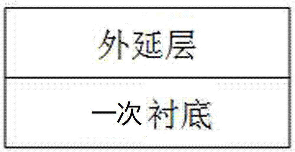
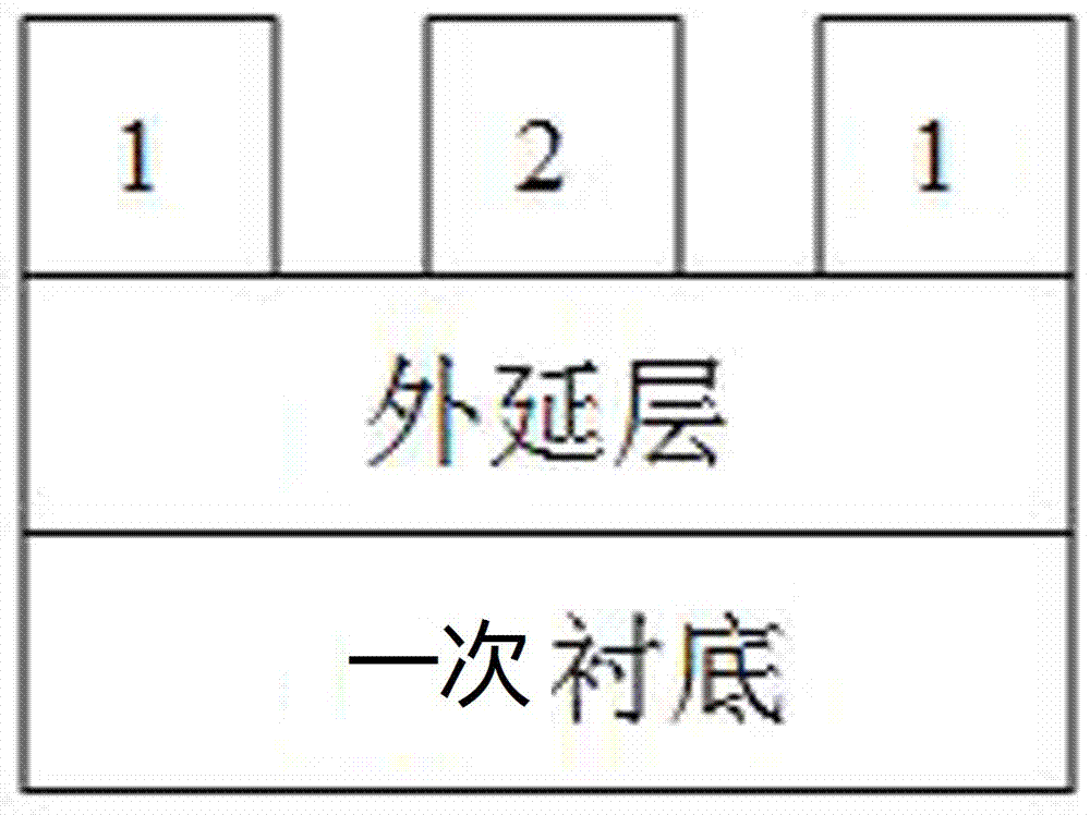
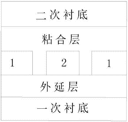
[0026] Since the growth of GaN materials generally uses sapphire, silicon carbide or silicon substrates, the dielectric constant of these substrate materials is about 10, and the loss for millimeter waves and terahertz waves is relatively large. If the growth substrate of the material is replaced by a substrate with a low dielectric constant such as quartz, the reflection loss and transmission loss can be reduced, and the performance of the modulator can be greatly improved. However, there is currently no millimeter-wave and terahertz direct modulation device based on substrate replacement technology in the world. This invention proposes a method for preparing a millimeter-wave and terahertz direct modulator that can realize substrate replacement technology, which can solve the current There is a problem of large loss in the modulator...


PUM

PropertyMeasurementUnit
Growth thicknessaaaaaaaaaa
Thicknessaaaaaaaaaa

Abstract

The invention discloses a millimeter-wave and terahertz-wave direct modulator and a fabrication method thereof, and belongs to the technical field of a semiconductor device. The millimeter-wave and terahertz-wave direct modulator comprises an epitaxial layer, wherein ohmic contactors are arranged at two sides of the epitaxial layer, a Schottky contactor is arranged between the two ohmic contactors, and quartz substrates are pasted on the formed ohmic contactors and the Schottky contactors by a chip bonding method to form a secondary substrate. By the millimeter-wave and terahertz-wave direct modulator, the reflection loss and the transmission loss of the device can be reduced, and a device with higher modulation depth is obtained.

Description

technical field [0001] The invention belongs to the technical field of semiconductor devices, in particular to a millimeter wave and terahertz wave direct modulator and a preparation method thereof. Background technique [0002] Si, GaAs, V 2 o 5 The terahertz direct modulation devices based on traditional semiconductor materials such as GaN and GaN are limited by the large dielectric constant of the material itself, so it is difficult to further improve the signal loss. In recent years, substrate replacement technology has developed rapidly in GaN semiconductor devices, which can replace the original high electromagnetic loss substrate of epitaxial materials with low loss substrate, so it is very developed in the field of millimeter wave and terahertz wave spatial modulation electronic devices Potential is currently a hot spot in the world. [0003] Since the growth of GaN materials generally uses sapphire, silicon carbide or silicon substrates, the dielectric constant o...

Claims


Application Information

Patent Timeline
IPC IPC(8): H01L29/778H01L21/335
CPCH01L29/66462H01L29/778H01L29/7786
Inventor 梁士雄王俊龙张立森杨大宝徐鹏赵向阳房玉龙冯志红
Owner THE 13TH RES INST OF CHINA ELECTRONICS TECH GRP CORP
Why Eureka
Try Eureka