
Liquid crystal display panel

A liquid crystal display panel, symmetry plane technology, applied in instruments, nonlinear optics, optics, etc., can solve problems such as abnormal display and uneven thickness of substrates, and achieve the effects of ensuring uniformity, reducing costs, and improving display performance.

Inactive Publication Date: 2016-01-13
TCL CHINA STAR OPTOELECTRONICS TECH CO LTD +1
View PDF5 Cites 10 Cited by
  • Summary
  • Abstract
  • Description
  • Claims
  • Application Information

AI Technical Summary

Problems solved by technology

In this way, the thickness of the box in the center of the substrate will be uneven, and the display will be abnormal.

Method used


Image

  • Liquid crystal display panel
  • Liquid crystal display panel
  • Liquid crystal display panel

Examples


Embodiment Construction

[0029] The present invention will be further described below in conjunction with accompanying drawing.

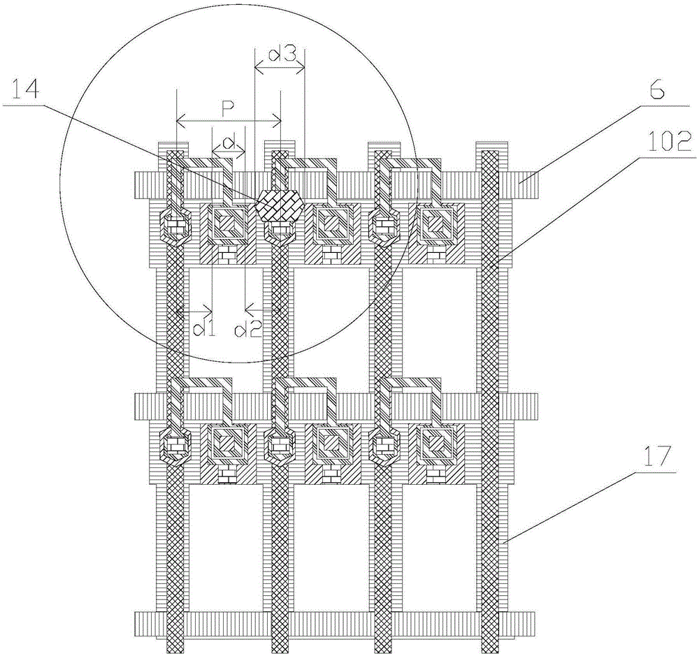
[0030] figure 2 A top view of a partial structure of a liquid crystal display panel in the prior art is shown. figure 2 It clearly shows that the array substrate of the liquid crystal display panel in the prior art includes a pixel unit 30 ( figure 2not marked). Each pixel unit 30 includes: a scanning line 6 extending along a first direction (ie, the left-right direction in the figure), a data line 102 extending along a second direction different from the first direction (ie, the up-down direction in the figure), and a selected pixel electrode (not shown in the figure); and a thin film transistor arranged between the data line 102 and the pixel electrode in a functionally connected manner. A black matrix 17 is provided at a position corresponding to the scan line 6 and the data line 102 for blocking light leakage. The pixel electrode may be disposed in an area surrou...


PUM


Abstract

The invention provides a liquid crystal display panel. An array substrate of the liquid crystal display panel comprises two or more pixel units, and each pixel unit comprises scanning lines, data lines, pixel electrodes and thin film transistors, wherein the scanning lines extend in the first direction, the data lines extend in the second direction different from the first direction, the thin film transistors are arranged between the data lines and the pixel electrodes in a mode of functional connection, and one or more parts of two adjacent pixel units are arranged in a mirror symmetry mode. The invention provides novel panel wire routing design. by means of the novel panel wire routing design, insulators can avert PLN via holes, and the phenomenon that the insulators slide into the PLN via holes in the process when liquid crystal cell pairing is conducted on the panel or a bending test is conducted is effectively prevented.

Description

technical field [0001] The invention relates to the field of display technology, in particular to a liquid crystal display panel. Background technique [0002] figure 1 A prior art liquid crystal display panel is shown. refer to figure 1 , in the region where the thin film transistor is arranged on the array substrate of the liquid crystal display panel: a light shielding structure 2 (LightShield, LS) for blocking light leakage is arranged on the first glass substrate 1 . A buffer layer 3 is covered on the light shielding structure 2 . A low temperature polysilicon layer 4 is disposed on the buffer layer 3 . The low temperature polysilicon layer 4 acts as a semiconductor channel in the transistor. The buffer layer 3 is used to block the electrical connection between the light shielding structure 2 and the low temperature polysilicon layer 4 . The low temperature polysilicon layer 4 is divided into multiple doped regions of different degrees, such as highly doped region...

Claims


Application Information

Patent Timeline
Patent Type & Authority Applications(China)
IPC IPC(8): G02F1/1362G02F1/1368
CPCG02F1/136227G02F1/136286G02F1/1368G02F1/13394G02F1/1339G02F1/133345G02F1/133512G02F1/133514
Inventor 王聪杜鹏
Owner TCL CHINA STAR OPTOELECTRONICS TECH CO LTD
Learn More