
Chip fracture image detection method

An image detection and chip technology, which is applied in semiconductor/solid-state device testing/measurement, electrical components, circuits, etc., can solve problems such as unsatisfactory use requirements and slow speed, and achieve high accuracy and fast response.

Inactive Publication Date: 2015-11-11
SHENZHEN HI TEST SEMICON EQUIP
View PDF4 Cites 0 Cited by
  • Summary
  • Abstract
  • Description
  • Claims
  • Application Information

AI Technical Summary

Problems solved by technology

Both methods have the same disadvantage: slow
Therefore, the current practical methods cannot meet the needs of the use

Method used


Image

  • Chip fracture image detection method
  • Chip fracture image detection method
  • Chip fracture image detection method

Examples


Embodiment Construction

[0019] refer to Figure 2-5 As shown, in order to have a better understanding and recognition of the present invention, now enumerate preferred embodiment and cooperate picture description as follows:

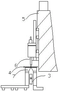
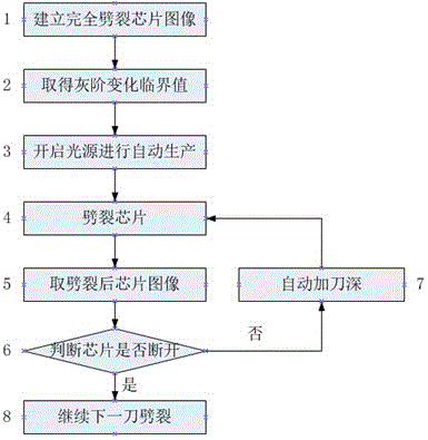
[0020] The present invention is an image detection chip unbroken method, which is applied to a wafer splitter 5 to determine whether the chip 4 is broken after the chip is split. The specific method steps include:

[0021] Step 1: Establish a completely split chip image, wherein, the chip image just after the chip 4 is completely split is collected by the image collector 3, and the acquisition of the chip image after the complete split needs to be deepened step by step until it is just split , at this time the image collected by the image collector 3 is the chip image after the complete splitting that we need.

[0022] Step 2: Obtain the critical value of the gray scale change, wherein, through the image processing unit, obtain the gray scale change critical value of the compl...


PUM


Abstract

The invention relates to a chip fracture image detection method. The chip fracture image detection method is applied to a wafer splitter and is used for judging whether chips are fractured after the chips are split. The method includes the following steps that: a completely split chip image is built; a gray scale change critical value is obtained; a light source is switched on, so that automatic production can be carried out; chips are split; and images of the split chip are obtained; and whether the chips are fractured is judged. According to the chip fracture image detection method of the invention, the images are acquired through an image acquisition device, and contrast processing is performed on the images, and therefore, whether the chips are fractured can be judged; and the image acquisition device has low requirements for resolution, and therefore, cost is low, and requirements of practical application can be satisfied.

Description

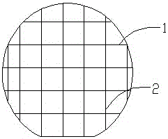
technical field [0001] The invention mainly relates to a wafer splitter for splitting a chip, in particular to a method for detecting whether a chip is broken after splitting. Background technique [0002] The wafer splitter is a device for splitting the chip 4 into crystal grains. Before the chip 4 is split, the horizontal cutting line 1 and the vertical cutting line 2 will be drawn with a laser cutting machine, but they are not cut, and about Three-fifths of the thickness are connected, and then the chip 4 is attached to the blue film (or white film) and covered with a protective film, and sent into the wafer splitter through the cassette for splitting operation. The chip 4 is split by the chopper unit 6 on the granting platform 7, wherein an image collector 3 is used, and the image collector 3 is used to monitor whether the positioning of the chip 4 is shifted, and judge whether the shift is Level repositioning to ensure splitting yield. [0003] When the chip is not ...

Claims


Application Information

Patent Timeline
Patent Type & Authority Applications(China)
IPC IPC(8): H01L21/66
CPCH01L22/12H01L22/24
Inventor 叶青山
Owner SHENZHEN HI TEST SEMICON EQUIP
Learn More