
CMOS (complementary metal oxide semiconductor) device and production method thereof

A technology of devices and stacked gates, which is applied in the field of CMOS semiconductor device preparation, can solve the problems of increasing the time required for the process, reducing the production efficiency, and failing to achieve compensation, etc., achieving the effects of low process implementation cost, improved device performance, and small process changes

Inactive Publication Date: 2015-06-10
SEMICON MFG INT (SHANGHAI) CORP
View PDF3 Cites 2 Cited by
  • Summary
  • Abstract
  • Description
  • Claims
  • Application Information

AI Technical Summary

Problems solved by technology

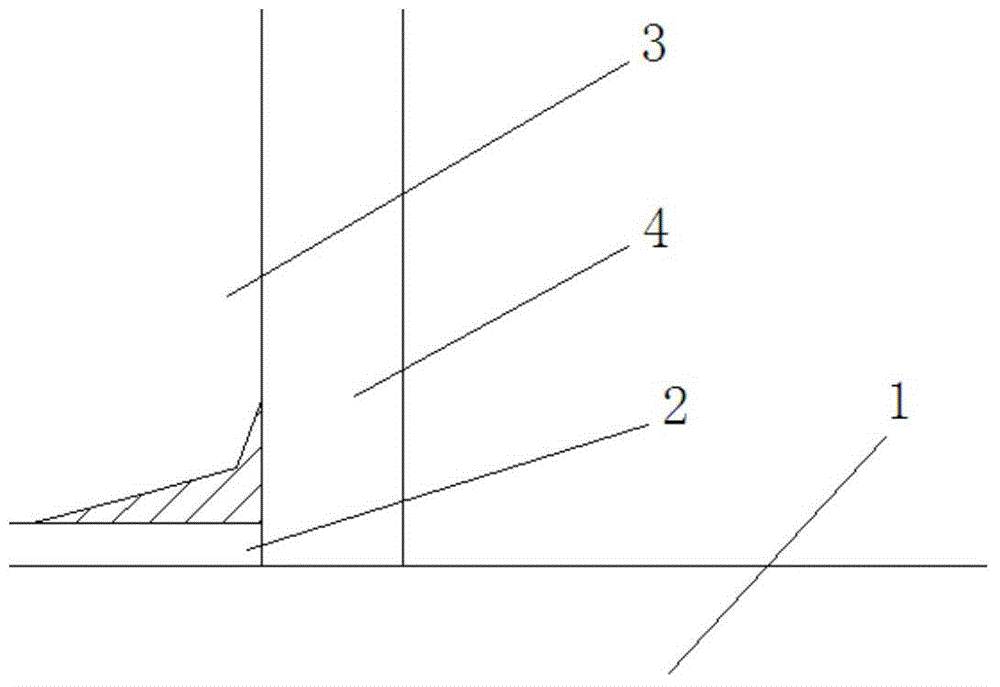
[0006] 1) Ion implantation is used to achieve compensation at the uneven thickness of the edge of the gate oxide layer. When using this method, the conditions of ion implantation (such as implant dose and energy) need to be precisely controlled. Once excessive, the device will be scrapped, and If it is too small, the compensation effect cannot be achieved, and the implanted ions in the process will also have an adverse effect on the gate structure;
[0007] 2) When preparing the sidewall of the oxide layer, an ISSG process I (nSituSteamGeneration, using on-site water vapor generation process) was added to reduce the polyoxidation reaction speed, but increasing the ISSG process will increase the time required for the process and reduce the production efficiency. At the same time, it will also have a certain impact on the side wall oxidation reaction.

Method used


Image

  • CMOS (complementary metal oxide semiconductor) device and production method thereof
  • CMOS (complementary metal oxide semiconductor) device and production method thereof
  • CMOS (complementary metal oxide semiconductor) device and production method thereof

Examples


Embodiment Construction

[0035] The specific embodiment of the present invention will be further described below in conjunction with accompanying drawing:

[0036] The present invention provides a kind of CMOS device preparation method, can refer to as shown in the figure, specifically comprise the following steps:

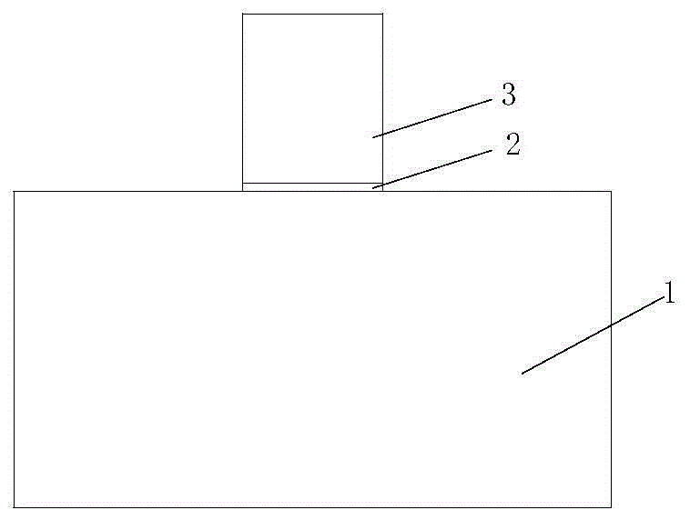
[0037] Step S1: Provide a bottom substrate 1, deposit a layer of gate oxide layer and a polysilicon layer on the substrate in sequence, then spin-coat a layer of photoresist on the surface of the polysilicon layer, and use a mask with a window pattern to expose and The development process forms an opening in the photoresist, and then uses the opening to etch down the polysilicon layer and the gate oxide layer to form a stacked gate; as image 3 As shown, the gate stack includes a gate oxide layer 2 at the bottom and a polysilicon gate 3 located on the gate oxide layer 2. In an embodiment of the present invention, the gate oxide layer is made of silicon dioxide (SiO 2 ).

[0038] Step S2...


PUM


Abstract

The invention provides a CMOS (complementary metal oxide semiconductor) device and a production method thereof. The production method includes the following steps: providing a bottom substrate, and producing a stacking gate electrode on the substrate, wherein the stacking gate electrode comprises a gate oxide at the bottom and a polysilicon gate positioned on the gate oxide; producing a gap wall to cover the lateral wall of the gate oxide, and continuing a side wall production process to form a side wall on the lateral wall of the gate electrode, wherein the side wall covers the gap wall and the lateral wall of the stacking gate electrode completely; performing ion implantation to form a source electrode and a drain electrode in the substrate. The CMOS device and the production method have the advantages that the gap wall is produced to cover a corner of the juncture between the gate oxide and the polysilicon gate completely, so that the beak phenomenon can be avoided effectively, defects, caused by bombarding ions, of the corner of the juncture between the gate oxide and the polysilicon gate are avoided during ion implantation of follow-up source and drain electrodes, and device performance is improved; change of the production process is small, and technical realization cost is low.

Description

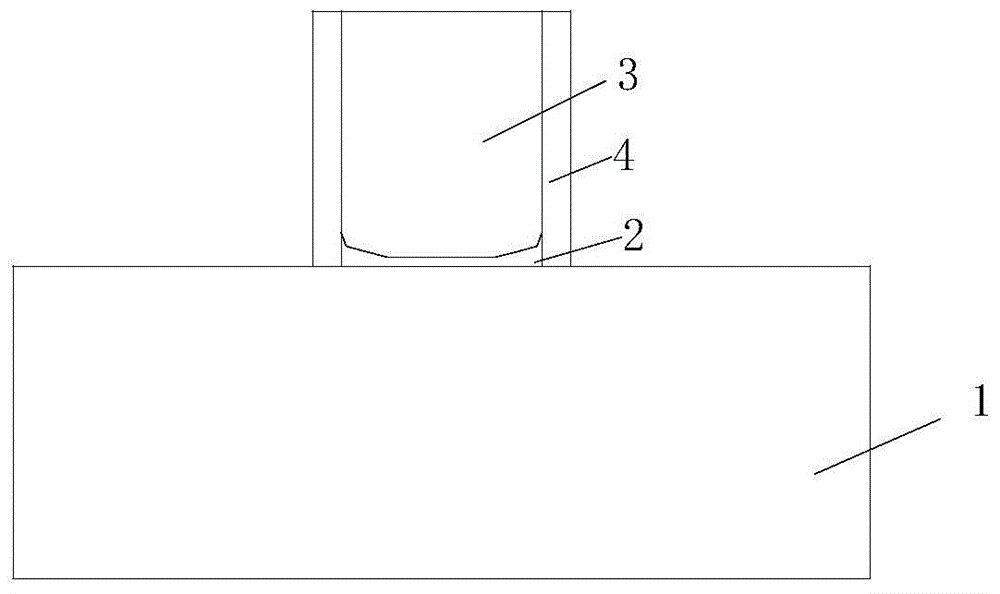
technical field [0001] The invention relates to the field of CMOS semiconductor device preparation, in particular to a CMOS device and a preparation method thereof. Background technique [0002] In devices manufactured by CMOS, the shape and thickness of the edge of the oxide layer on the sidewall of the polysilicon gate has become a very important issue in the field of CMOS manufacturing. [0003] Can refer to Figure 1-2 As shown, in the CMOS manufacturing process, generally, the gate oxide layer 2 and the polysilicon gate 3 are successively formed on the substrate 1 to form the stacked gate, and then the spacer 4 is formed on the sidewall of the stacked gate. However, when preparing the sidewall 4 of the gate oxide layer, since the diffusion of oxygen is an isotropic process, as the oxidation continues, the gate oxide layer 2 is easy to form diffusion at the corner of the junction with the polysilicon gate 3, and then As a result, the thickness of the oxide layer near th...

Claims


Application Information

Patent Timeline
IPC IPC(8): H01L27/092H01L21/8238H01L29/49
Inventor 赵猛
Owner SEMICON MFG INT (SHANGHAI) CORP
Learn More