
Method for manufacturing semiconductor element with metal gate

A metal gate and semiconductor technology, which is applied in semiconductor/solid-state device manufacturing, semiconductor devices, electrical components, etc., can solve problems such as complex back gate technology, achieve good hole filling ability, novel process design, and increase reliability Effect

Active Publication Date: 2016-12-14
UNITED MICROELECTRONICS CORP
View PDF8 Cites 0 Cited by
  • Summary
  • Abstract
  • Description
  • Claims
  • Application Information

AI Technical Summary

Problems solved by technology

However, because the gate-last process is quite complicated and requires multiple processes to complete, manufacturers are currently striving to simplify the process of forming metal gates.

Method used


Image

  • Method for manufacturing semiconductor element with metal gate
  • Method for manufacturing semiconductor element with metal gate
  • Method for manufacturing semiconductor element with metal gate

Examples


Embodiment Construction

[0029] In order to enable those skilled in the art of the present invention to further understand the present invention, several preferred embodiments of the present invention are enumerated below, together with the accompanying drawings, to describe in detail the composition and desired effects of the present invention.

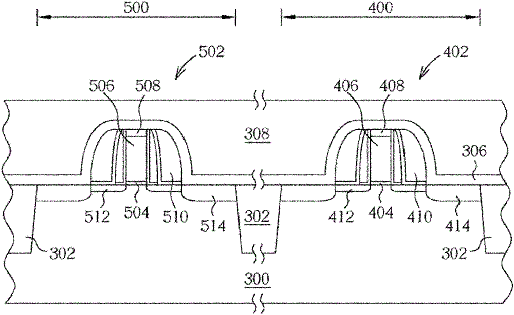
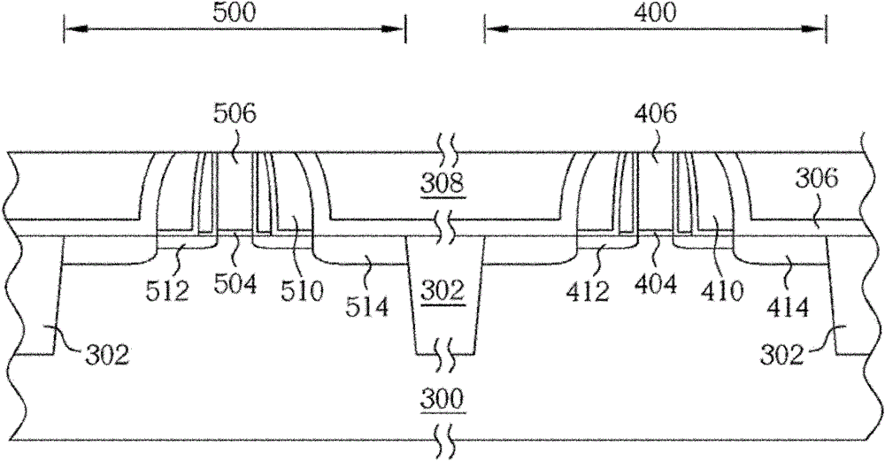
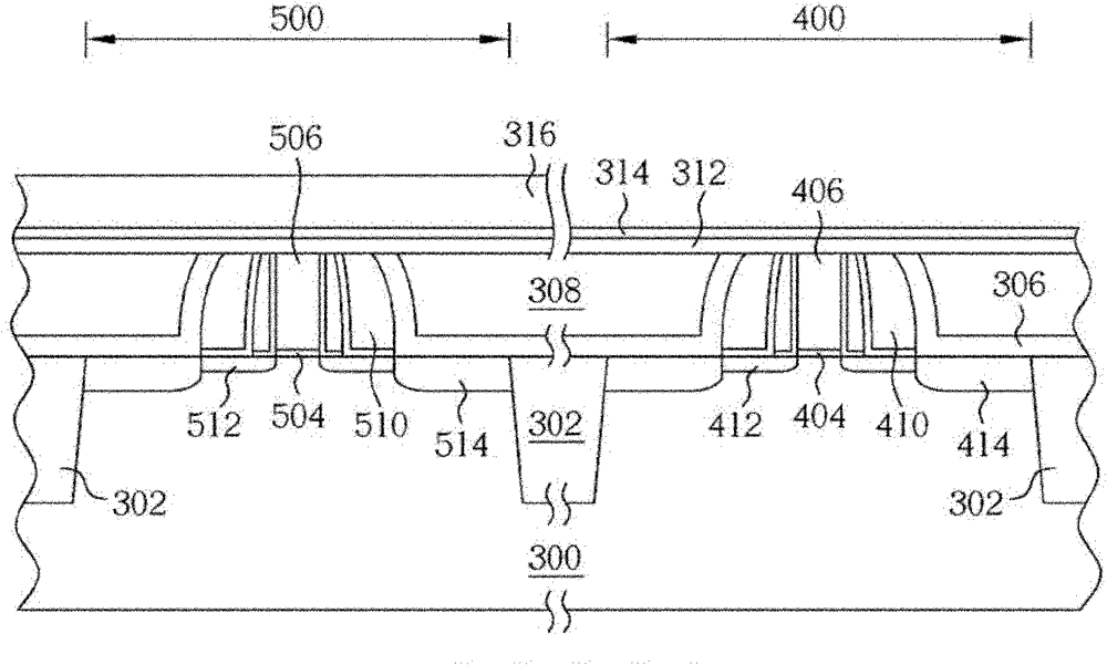
[0030] Please refer to Figure 1 to Figure 12 , is a schematic diagram of a method for fabricating a semiconductor device with a metal gate in the first embodiment of the present invention. First, a substrate 300 is provided, such as a silicon substrate, a silicon-containing substrate, or a silicon-on-insulator (SOI) substrate. The substrate 300 has a plurality of shallow trench isolations (STIs) 302 . The first active region 400 and the second active region 500 which are electrically insulated from each other can be defined by the region surrounded by the shallow trench isolation 302 . Next, the first conductive type transistor 402 and the second conductiv...


PUM


Abstract

The invention provides a method for manufacturing a semiconductor element with a metal gate. First provide the base. The substrate includes transistors of the first conductivity type and transistors of the second conductivity type. The transistor of the first conductivity type includes a first sacrificial gate, and the transistor of the second conductivity type includes a second sacrificial gate. Then remove the first sacrificial gate to form a first trench, and form a first metal layer and a first material layer in the first trench. The first metal layer and the first material layer are planarized. Then the second sacrificial gate is removed to form a second trench, and a second metal layer and a second material layer are formed in the second trench. Finally, the second metal layer and the second material layer are planarized.

Description

technical field [0001] The invention relates to a manufacturing method of a semiconductor element with a metal gate. Background technique [0002] In the known semiconductor industry, polysilicon is widely used in semiconductor devices such as metal-oxide-semiconductor (MOS) transistors as a standard gate material choice. However, as the size of MOS transistors continues to shrink, traditional polysilicon gates have problems such as boron penetration (boron penetration) that leads to device performance degradation and unavoidable depletion effects, making the equivalent gate dielectric The thickness of the electrical layer increases and the capacitance of the gate decreases, which in turn leads to the decline of the driving ability of the device and other difficulties. Therefore, the semiconductor industry is trying to use new gate materials, such as using work function metals to replace the traditional polysilicon gates, as a control electrode that matches the high-k (High...

Claims


Application Information

Patent Timeline
Patent Type & Authority Patents(China)
IPC IPC(8): H01L21/8238H01L21/28
Inventor 廖柏瑞蔡宗龙林建廷徐韶华吕水烟周珮玉陈信琦廖俊雄蔡尚元杨建伦蔡腾群林俊贤
Owner UNITED MICROELECTRONICS CORP
Learn More