ESD (Electronic Static Discharge) protection device
A technology of ESD protection and binding posts, which is applied in the direction of emergency protection circuit devices, circuit devices, emergency protection circuit devices for limiting overcurrent/overvoltage, etc., which can solve problems such as inability to protect internal circuits and high trigger voltage, and achieve protection Internal circuit, the effect of eliminating excessive voltage
- Summary
- Abstract
- Description
- Claims
- Application Information
AI Technical Summary
Problems solved by technology
Method used
Image
Examples
no. 1 example
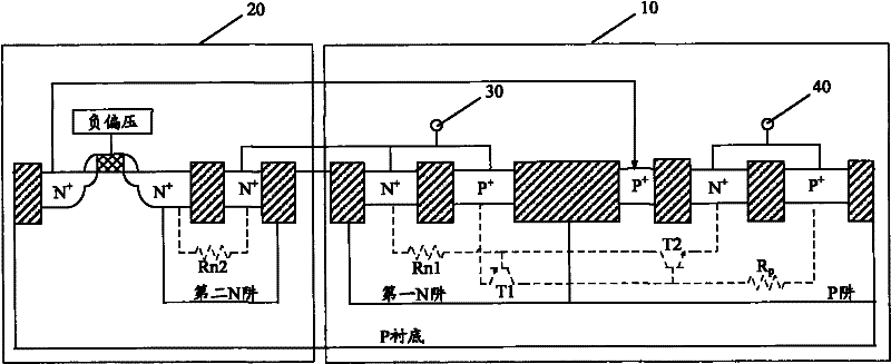
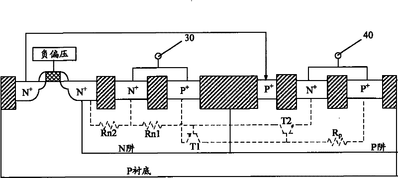
[0022] The ESD protection device of this embodiment is such as figure 2 As shown, the device is located on a P substrate, including a thyristor 10 and a depletion NMOS transistor 20 .
[0023] The thyristor 10 includes a parasitic PNP transistor T1 and a parasitic NPN transistor T2; the emitter of the parasitic PNP transistor T1 is connected to the anode terminal 30, and its base is connected to the anode terminal 30 through the parasitic resistance Rn1 of the first N well; The emitter of the parasitic NPN transistor T2 is connected to the cathode terminal 40, and its base is connected to the cathode terminal 40 through the P well parasitic resistance Rp; the thyristor 10 also includes a P well located in the P well. + well contact, the P + The well contact is connected to the base of the parasitic NPN transistor T2. like figure 2 Shown, preferably, the P + well contact located on the first N-well of the thyristor 10 P + and P-well N + between.
[0024] The gate of th...
no. 2 example
[0035] The ESD protection device of this embodiment is as follows Figure 4 As shown, the device is located on an N substrate and includes a thyristor 50 and a depletion-mode PMOS transistor 60 .
[0036] The thyristor 50 includes a parasitic PNP transistor T3 and a parasitic NPN transistor T4; the emitter of the parasitic PNP transistor T3 is connected to the anode terminal 30, and its base is connected to the anode terminal 30 through the N-well parasitic resistance Rn; the parasitic The emitter of the NPN transistor T4 is connected to the cathode terminal 40, and its base is connected to the cathode terminal 40 through the parasitic resistance Rp1 of the first P-well; the thyristor 50 further includes a P-well located in the first P-well + well contacts, the P + The well contact is connected to the base of the parasitic NPN transistor T4.
[0037] The gate of the PMOS transistor 60 is positively biased; the drain of the PMOS transistor 60 is connected to the anode termina...
PUM
 Abstract
Description
Claims
Application Information
 - R&D Engineer
- R&D Manager
- IP Professional
- Industry Leading Data Capabilities
- Powerful AI technology
- Patent DNA Extraction
Browse by: Latest US Patents, China's latest patents, Technical Efficacy Thesaurus, Application Domain, Technology Topic, Popular Technical Reports.
© 2024 PatSnap. All rights reserved.Legal|Privacy policy|Modern Slavery Act Transparency Statement|Sitemap|About US| Contact US: help@patsnap.com


