
Multi-sectorization shallow junction low-temperature semiconductor structure with differ doping concentration and high disruptive voltage as well as manufacturing method thereof

A technology with high breakdown voltage and doping concentration, applied in semiconductor devices, electric solid devices, circuits, etc., can solve the problems of complex design, incompatibility, thick dielectric thickness, etc., reduce complexity and difficulty, and have a wide range of applications Effect

Active Publication Date: 2008-12-24
NO 24 RES INST OF CETC
View PDF0 Cites 0 Cited by
  • Summary
  • Abstract
  • Description
  • Claims
  • Application Information

AI Technical Summary

Problems solved by technology

[0005] Aiming at the above problems that the junction termination technology with higher breakdown is complex in design, relies on deeper junction depth, thicker dielectric thickness, and is incompatible with the trend of modern deep submicron low temperature shallow junction technology, the present invention provides a different doped A low-temperature semiconductor structure and manufacturing method with multiple dopant concentrations and high breakdown voltage shallow junctions, and a new junction termination technology that conforms to the development trend of modern planar technology

Method used


Image

  • Multi-sectorization shallow junction low-temperature semiconductor structure with differ doping concentration and high disruptive voltage as well as manufacturing method thereof
  • Multi-sectorization shallow junction low-temperature semiconductor structure with differ doping concentration and high disruptive voltage as well as manufacturing method thereof
  • Multi-sectorization shallow junction low-temperature semiconductor structure with differ doping concentration and high disruptive voltage as well as manufacturing method thereof

Examples


Embodiment Construction

[0028] The specific implementation of the present invention is not limited to the semiconductor device described below, but also other semiconductor devices that can improve the breakdown voltage by adopting various similar methods that can meet the structural requirements according to the structural core and design spirit of this method.

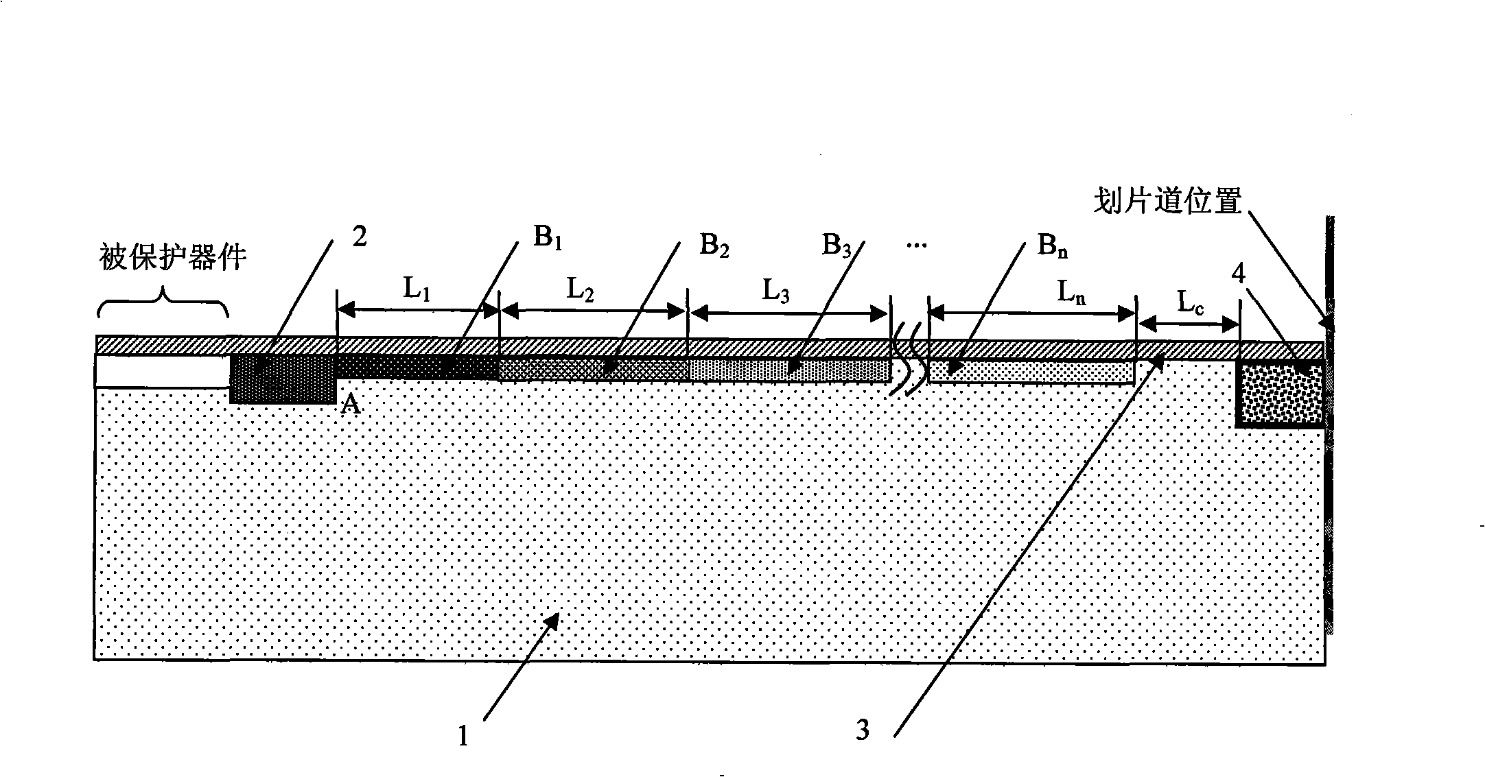
[0029] The main structure of the junction termination technology proposed by this method is as follows: figure 1 As shown, its structure includes semiconductor material 1, main diffusion junction 2, partition withstand voltage layer B 1 、B 2 、B 3 until B n (where n≥2) and the depletion termination region 4 and the dielectric layer 3 . figure 1 It also schematically shows the "protected device" in the upper left corner and the "scribing lane position" on the right side of the figure. Generally, the junction termination of the protected device is symmetrical, and figure 1 Take the symmetric structure of the junction terminal section on t...


PUM


Abstract

The invention relates to a high breakdown voltage shallow-junction low-temperature semiconductor structure with different doping concentrations and a plurality of sub-areas and a manufacturing method. The structure comprises a semiconductor material, a main diffused junction, n pressure-resist layers B1 to Bn (n is larger than or equal to 2), an exhaustion and termination area and a dielectric layer, wherein, the main diffused junction, the n pressure-resist layers B1 to Bn and the exhaustion and termination area are positioned in the semiconductor material, the conduction types of the main diffused junction and the voltage withstand layer are opposite to that of the semiconductor material, and the conduction types of the exhaustion and termination area is identical to that of the semiconductor material. The structure can ensure that the breakdown voltage of the main diffused junction can be increased by more than 30 percent, and can ensure that the breakdown voltage of the main diffused junction can be more than 80 percent of the maximum avalanche breakdown voltage of the ideal parallel planar junction of the semiconductor material. The structure can be applied to the terminal of the semiconductor device with scores of or thousands of volts, and particularly the structure and the manufacture of the high-voltage semiconductor device and integrated circuit.

Description

(1) Technical field [0001] The present invention relates to a structure and manufacturing method of a semiconductor device and an integrated circuit, in particular to a structure and a manufacturing method of a shallow-junction low-temperature semiconductor device with different doping concentrations and multiple partitions and a high breakdown voltage, which is suitable for the structure and manufacturing of a high-voltage semiconductor device and an integrated circuit . (2) Background technology [0002] In the structure and manufacture of high-voltage semiconductor devices and integrated circuits, ensuring that the device has sufficient voltage withstand capability is a prerequisite for the device to work normally. The manufacture of modern semiconductor devices and integrated circuits generally adopts the method of doping impurities from different regions on the surface to form devices, and it is difficult to do any region and concentration within the semiconductor mater...

Claims


Application Information

Patent Timeline
Patent Type & Authority Applications(China)
IPC IPC(8): H01L29/06H01L27/04
Inventor 谭开洲胡永贵刘勇欧宏旗唐昭焕
Owner NO 24 RES INST OF CETC
Learn More