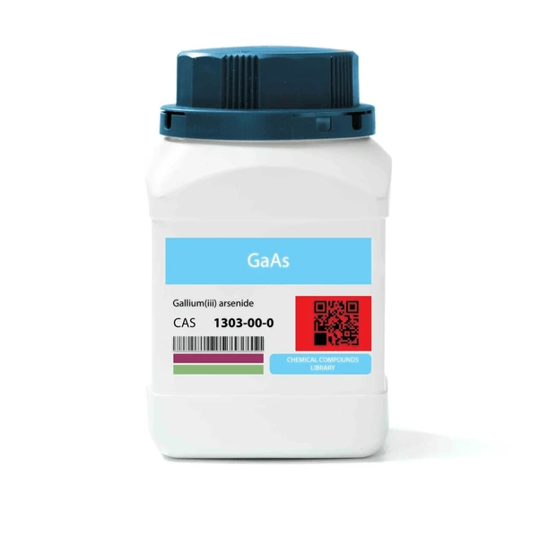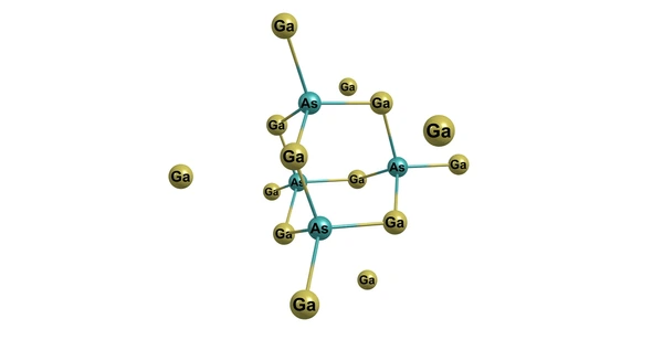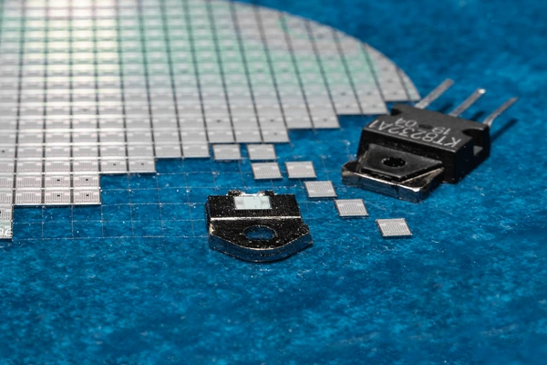
What Is Gallium Arsenide?
Gallium Arsenide (GaAs) is a compound semiconductor material composed of gallium and arsenic elements. It is a direct bandgap semiconductor with a bandgap energy of 1.42 eV at room temperature, making it suitable for optoelectronic applications. GaAs exhibits superior electronic properties compared to silicon, including higher electron mobility (up to 6 times higher than Si), higher saturated electron velocity, and semi-insulating properties. These properties make GaAs an attractive material for high-frequency and high-speed electronic devices.

Key Properties of Gallium Arsenide
- Direct Bandgap: GaAs has a direct bandgap of 1.42 eV at room temperature, allowing efficient emission and absorption of light, making it suitable for optoelectronic devices like lasers and photodetectors.
- High Electron Mobility: GaAs has a high electron mobility (around 8,500 cm²/V·s), which is about six times higher than silicon, enabling high-speed operation in electronic devices.
- High Breakdown Voltage: GaAs has a high breakdown voltage (around 5×10^5 V/cm), allowing it to withstand high electric fields and operate at high power levels.
- Wide Operating Frequency Range: GaAs devices can operate from 30 MHz to millimeter-wave frequencies as high as 250 GHz, making them suitable for various communication and radar applications.
- Thermal Conductivity: GaAs has a relatively high thermal conductivity, which is essential for dissipating heat in high-power and high-frequency devices.
Production of Gallium Arsenide
- Liquid Encapsulated Czochralski (LEC): This method involves melting GaAs in a crucible covered by a liquid encapsulant (e.g., B2O3) to prevent arsenic loss. The crystal is then pulled from the melt, allowing control over crystal diameter and doping levels.
- Vertical Bridgman (VB): In this method, a sealed ampoule containing GaAs is heated and slowly cooled from one end, allowing the crystal to solidify directionally.
- Vertical Gradient Freeze (VGF): Similar to VB, but the ampoule is cooled by moving a gradient freeze zone along its length, allowing better control over crystal quality and doping profiles.
- Electrospinning: A novel method for producing GaAs nanofibers by electrospinning a gallium nitrate/polymer solution in the presence of arsenic vapor, resulting in a polymer shell with a GaAs nanofiber core.
Advantages of Gallium Arsenide Over Silicon
Material Properties
- GaAs has a direct bandgap, allowing for efficient light emission and absorption, making it superior for optoelectronic devices like lasers and photodetectors.
- GaAs has higher electron mobility (up to 6 times) compared to Si, enabling faster switching speeds and higher-frequency operation in electronic devices.
Device Performance
- GaAs-based transistors and integrated circuits can operate at much higher frequencies (up to millimeter-wave range) than Si-based counterparts, crucial for 5G and radar applications.
- GaAs solar cells have higher conversion efficiency (up to 29%) compared to Si cells (around 20%), making them attractive for space and concentrated photovoltaic applications.
Thermal and Power Handling
- GaAs has a wider bandgap (1.42 eV) than Si (1.12 eV), allowing operation at higher temperatures and voltages without excessive leakage currents.
- GaAs devices can handle higher power densities and operate at higher voltages, enabling more compact and efficient power electronics.
Integration and Cost
- GaAs can be grown on larger Si wafers using epitaxial techniques, leveraging the cost advantages of Si substrates while retaining GaAs’s superior properties.
- Techniques like releasable multilayer epitaxial assemblies enable large-area integration of GaAs devices on foreign substrates like glass, plastic, or Si, reducing costs.
Challenges of Using Gallium Arsenide
- Higher Production Cost: GaAs substrates and manufacturing processes are significantly more expensive than Si, limiting their widespread adoption in cost-sensitive applications.
- Mechanical Properties: GaAs has relatively weaker mechanical properties compared to Si, requiring careful handling and packaging. However, nanostructured forms like GaAs nanofibers can potentially improve mechanical properties.
- Substrate Size Limitations: Large-diameter GaAs substrates (e.g., >205 mm) are challenging to produce, limiting economies of scale compared to Si.

Applications of Gallium Arsenide
Optoelectronic Devices and Applications
GaAs is widely used in optoelectronic devices due to its direct bandgap and high electron mobility. Key applications include:
- Laser diodes for fiber optic communications, CD/DVD players, and laser printers
- Light-emitting diodes (LEDs) for displays, indicators, and solid-state lighting
- Photodetectors and solar cells for optical communications and photovoltaics
- Vertical-cavity surface-emitting lasers (VCSELs) for data communications and sensing
High-Speed Electronics and RF Applications
The high electron mobility and saturation velocity of GaAs make it suitable for high-frequency and high-speed electronic devices:
- Microwave and millimeter-wave integrated circuits for radar, satellite communications
- High electron mobility transistors (HEMTs) for power amplifiers in wireless communications
- Monolithic microwave integrated circuits (MMICs) for radar, satellite, and terrestrial communications
Power Electronics
GaAs has a higher breakdown voltage compared to silicon, enabling power device applications:
- Power amplifiers for cellular base stations and broadcast transmitters
- Power switching devices for power supplies and motor controls
Thin Film Transistors (TFTs)
GaAs is explored as a channel material in TFTs for display and imaging applications due to its high mobility:
- Active-matrix liquid crystal displays (AMLCDs) and organic LED displays
- Flat panel image sensors for medical and industrial imaging
Emerging Applications
- GaAs nanowires for nanoelectronics and optoelectronics
- GaAs as a lithium-ion battery anode material with high capacity
- GaAs chemical sensors for potentiometric detection of metal ions
Application Cases
| Product/Project | Technical Outcomes | Application Scenarios |
|---|---|---|
| Thin Film Transistors Applied Materials, Inc. | Incorporating GaAs-based layers enhances electrical performance and speed by offering high electron mobility and stability. | Thin film transistor devices for improved performance and reliability. |
| High Electron Mobility Transistors (HEMTs) Wolfspeed, Inc. | Forming gate electrodes with protective layers and optimized profiles addresses current collapse and capacitance issues, improving high-frequency performance. | High-power, high-frequency applications like radar, satellite communications. |
| High-Frequency Transistors MACOM Technology Solutions Holdings, Inc. | Self-aligning source/drain implants using masking gates ensures precise placement near the gate metal, enhancing performance. | High-frequency devices for wireless communications and other RF applications. |
| Power Semiconductor Packages Semiconductor Components Industries LLC | Dual-sided cooling and direct-bonded metal substrates achieve efficient thermal dissipation and electrical isolation for high-power ratings. | High-voltage, high-power applications requiring effective thermal management. |
| GaAs Ohmic Contacts The Regents of the University of California | Co-implantation of N and Group VI donors enhances n-type doping, achieving low resistivity and improved surface morphology. | Fabrication of reliable and efficient n-type GaAs ohmic contacts. |

Latest Technical Innovations in Gallium Arsenide
Novel GaAs Substrate Surface Treatment
A new process has been developed for producing surface-treated GaAs substrates with improved surface quality and homogeneity. The key steps involve:
- Dry oxidation treatment of the GaAs surface using UV radiation and/or ozone gas
- Contacting the surface with a liquid medium
- Marangoni drying of the substrate.This process enables precise optical characterization and quantification of surface properties using techniques like ellipsometric lateral substrate mapping.
GaAs Material Synthesis and Nanostructures
Advances have been made in synthesizing novel GaAs nanostructures with unique properties:
- GaN/AlGaN/AlN/GaN high electron mobility transistor (HEMT) heterostructures for high-power, high-frequency electronics
- GaAs/AlGaAs core-shell nanowires with tunable electronic properties
- Self-assembled GaAs/AlGaAs quantum dots for optoelectronics
Breakthroughs in epitaxial growth techniques like molecular beam epitaxy (MBE) and metal-organic chemical vapor deposition (MOCVD) have enabled precise control over composition, doping, and nanostructure dimensions.
GaAs Defect Engineering
Controlling and engineering defects in GaAs has emerged as a powerful approach to tailor its properties:
- Introduction of isoelectronic impurities (e.g., N, Bi) modifies the bandgap and spin properties
- Generation of self-interstitials and vacancies via ion implantation for quantum computing applications
- Controlled formation of anti-phase boundaries for novel electronic and photonic devices
To get detailed scientific explanations of gallium arsenide, try Patsnap Eureka.

Learn more
Hypertonic vs. Hypotonic vs. Isotonic: What’s the Difference?
Acetophenone: A Key Compound in Fragrance and Industry
Magnesium Nitrate: Key Uses, Definition, and Innovations
