Introduction
P-Type and N-Type semiconductors play a critical role in modern electronics and materials science. These essential components are the building blocks for devices like diodes, transistors, and solar cells. Understanding their unique properties and functions is key to advancing semiconductor technologies. Whether you’re designing cutting-edge electronics or working with photovoltaic systems, mastering the mechanisms behind these semiconductors is crucial for innovation in the tech industry.
What is a P-Type Semiconductor?
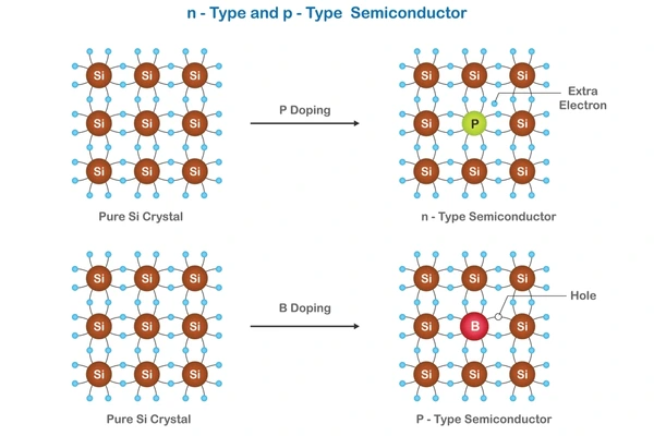
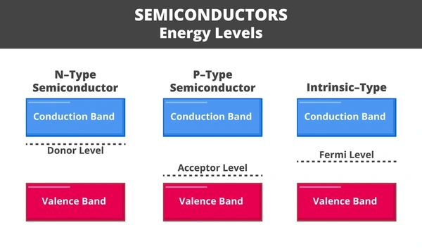
P-Type semiconductors are a key type of semiconductor where holes, or the absence of electrons, act as charge carriers. These holes move in the opposite direction of electrons, carrying positive charge. P-Type semiconductors are made by doping materials like silicon or germanium with trivalent elements, such as boron, gallium, or indium. This process creates acceptor levels just above the valence band, allowing holes to form when electrons are thermally excited.
When trivalent dopants like boron are introduced to a semiconductor, they replace silicon atoms in the crystal lattice. This replacement creates a hole, or an electron deficiency, in the valence band. As electrons from neighboring atoms fill the hole, the hole moves through the lattice. This movement of holes generates electrical conductivity in P-Type semiconductors.
What is an N-Type Semiconductor?
N-type semiconductors are materials where electrons serve as the majority charge carriers. These semiconductors form by doping pure materials, such as silicon, with elements that have more valence electrons. The doping process introduces free electrons, which boosts the material’s electrical conductivity.
To create N-type semiconductors, manufacturers add impurities like phosphorus, arsenic, or antimony to the base material. These elements have five valence electrons, one more than silicon. When silicon receives phosphorus doping, the phosphorus atoms donate free electrons to the conduction band. This additional electron improves the material’s ability to conduct electricity.

How P-Type and N-Type Semiconductors are Doped
The doping process employs various techniques, each with specific advantages and challenges:
Chemical Vapor Deposition (CVD)
CVD frequently dopes semiconductors, particularly materials like diamond. Boron is used for P-type doping, while phosphorus serves N-type doping. However, issues such as deep impurity levels and defects may impact carrier concentration and mobility.
Ion Implantation
Ion implantation bombards the semiconductor with dopant ions, offering precise control over concentration and distribution. This method is common in transistor fabrication for creating different doped regions, like source and drain areas.
Coevaporation and Spin Coating
In organic semiconductors, coevaporation and spin coating achieve doping. N-type dopants like Cs2CO3 and FeCl3, and P-type dopants like P3HT are commonly used. Techniques such as evaporative spray deposition enhance doping efficiency.
Selective Electroplating
Selective electroplating enables plating on semiconductor surfaces. This method uses direct current (d.c.) or periodic reverse (PR) plating voltages to control doping precisely.
Molecular Doping
Molecular doping transfers charge to the semiconductor using molecular dopants. For example, F4TCNQ acts as an electron acceptor for P-type doping in halide perovskites, effectively tuning carrier properties.

Key Differences Between P-Type and N-Type Semiconductors
Charge Carriers and Conductivity
P-type semiconductors primarily use holes as charge carriers, created by electron loss, making the material positively charged. N-type semiconductors use electrons as charge carriers, which are abundant due to donor impurities that add extra electrons.
Doping Elements
P-type semiconductors are doped with trivalent elements like aluminum (Al), gallium (Ga), and indium (In), creating holes. N-type semiconductors, on the other hand, are doped with pentavalent elements like phosphorus (P), arsenic (As), and antimony (Sb), adding extra electrons.
Energy Levels and Fermi Level Position
In P-type semiconductors, the acceptor energy levels are close to the valence band. In N-type semiconductors, donor energy levels are near the conduction band. The Fermi level in P-type semiconductors lies between the acceptor level and valence band, while in N-type semiconductors, it’s between the donor level and conduction band.
Majority and Minority Carriers
In P-type semiconductors, holes are the majority carriers, and electrons are the minority carriers. In N-type semiconductors, electrons are the majority carriers, and holes are the minority carriers. This difference affects the semiconductor’s electrical properties.
P-N Junction Formation
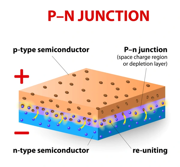
A P-N junction forms when a P-type region is placed next to an N-type region. This junction controls current flow and is essential for diodes, transistors, and photovoltaic cells.

Applications of P-Type Semiconductors
- Diodes and Transistors: P-type semiconductors combine with N-type semiconductors to form p-n junctions, which are essential for diodes and BJTs.
- Photovoltaic Cells: P-type semiconductors play a key role in solar cells by forming p-n junctions that convert light into electricity. Materials like Cu2O and NiO serve this purpose.
- Light Emitting Diodes (LEDs): P-type materials facilitate electron-hole recombination in LEDs, which produces light.
- Sensors: P-type semiconductors work in chemical and biological sensors due to their sensitivity to environmental changes.
Applications of N-Type Semiconductors
- Organic Electrochemical Transistors (OECTs): N-type semiconductors are vital in OECTs, used for bioelectronics like biosensors and neuromorphic devices.
- Organic Thin-Film Transistors (OTFTs): N-type polymers are key in OTFTs, which power flexible electronics and displays.
- Polymer Solar Cells (PSCs): N-type semiconductors act as electron acceptors in PSCs, boosting solar energy conversion efficiency.
- Thermoelectric Devices: N-type semiconductors are used in thermoelectric devices that convert temperature differences into electrical voltage, ideal for power and cooling applications.
Complementary Use of Both Semiconductors
Field Effect Transistors (FETs): Both materials work together in FETs, creating efficient current channels and improving overall performance.
Complementary Metal-Oxide-Semiconductor (CMOS) Technology: CMOS technology integrates both materials to produce low-power, high-performance circuits in processors and memory devices.
Photocatalysts: P-N type semiconductor composites are used in environmental applications like pollutant degradation and hydrogen production through water splitting.
FAQ
Why are these semiconductors important?
- These semiconductors are crucial for the operation of electronic devices like diodes, transistors, and solar cells, enabling controlled flow of electrical current.
What is the role of doping in semiconductors?
- Doping is the process of adding small amounts of impurity elements to semiconductors to control their electrical properties—creating either P-type or N-type semiconductors based on the added material.
To get detailed scientific explanations of P-Type and N-Type semiconductors, try Patsnap Eureka.

