
What Is OLED Burn-In?
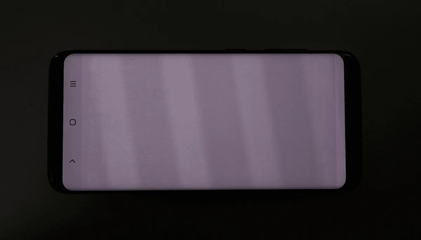
OLED burn-in is a common concern for users of organic light-emitting diode (OLED) displays. This phenomenon occurs when static images or bright areas are displayed for prolonged periods, causing certain pixels to degrade faster than others. Over time, this can lead to visible discoloration or uneven brightness, creating permanent visual artifacts on the screen.
While OLED technology offers incredible picture quality with deep blacks and vibrant colors, understanding and preventing burn-in is essential for maintaining the longevity and performance of your display. In this article, we’ll explore what causes OLED burn-in, how to minimize the risks, and whether it’s a significant issue for modern OLED screens.
Signs and Symptoms of OLED Burn-In
Screen Burn (Burn-in):
- Permanent degradation of display components (e.g., OLED organic pixels, plasma phosphors) due to prolonged static content exposure, causing irreversible luminance/color shifts.
- Mechanism: Cumulative deterioration of emissive materials (e.g., OLED blue subpixels degrade faster due to higher energy requirements) . For phosphor-based displays (CRT, plasma), uneven aging of phosphor coatings creates permanent “ghosts”.
- Critical Threshold: Depends on cumulative exposure (e.g., 10 hours of static content at 100% brightness may cause measurable degradation in OLEDs ).
1. Persistent Brightness Differences
- Uneven Pixel Wear: Pixels showing static or repeated images may become dimmer than surrounding areas.
- Impact of Prolonged Intensity: Static visuals degrade specific pixels faster, creating noticeable brightness inconsistencies.
2. Color Drift
- Altered Hue: Colors in static images may shift, appearing less accurate or adopting a different tint.
- Uneven Material Wear: This occurs due to the uneven degradation of the organic compounds in the display.
3. Visible Marks or Ghosting
- Lingering Shadows: Static images may leave faint marks, known as ghosting, when the screen displays new content.
- Severity: The prominence of these marks depends on the duration and intensity of the static visuals.
Symptoms of Screen Degradation
1. Non-Uniform Brightness
- Uneven Illumination: Certain screen areas may display varying brightness levels, especially noticeable with solid colors.
2. Image Retention
- Lingering Visuals: Static content can leave temporary impressions, appearing faintly on other displayed images.
3. Reduced Lifespan
- Pixel Degradation: Prolonged use of repetitive images accelerates wear, reducing the screen’s overall quality and longevity.
What’s the difference between screen burn and image retention?
| Parameter | Screen Burn | Image Retention |
|---|---|---|
| Permanence | Irreversible | Reversible |
| Root Cause | Material degradation (OLED/phosphor) | Electrical/thermal transients |
| Mitigation | Pixel shifting , luminance adjustment , screen savers | Automatic compensation cycles , temperature control |
| Industry Relevance | Critical for OLED/plasma R&D | LCD/electrophoretic display focus |
Understanding the Causes and Prevention of OLED Burn-In
Curious about OLED burn-in? Eureka Technical Q&A explains the causes behind OLED burn-in, such as prolonged static images and high brightness settings. Discover effective prevention techniques, including screen savers, pixel shifting, and proper usage habits, to maintain the quality and longevity of your OLED displays.
Causes of OLED Burn-In
- Static Content Display: One major cause of OLED burn-in is displaying static images for long periods. When certain pixels stay lit for too long, they degrade faster, leading to visible burn-in patterns.
- High Brightness Levels: Operating OLED displays at high brightness can speed up degradation. The heat from high brightness levels causes uneven wear on pixels, contributing to burn-in.
- Temperature Variations: Temperature changes affect OLED performance, especially in devices like vehicle displays. Fluctuating temperatures can lead to uneven degradation and burn-in.
- Intrinsic Material Degradation: The organic materials in OLEDs naturally degrade over time. Factors like moisture, oxygen, and electrical stress cause luminance loss and burn-in.
Prevention of OLED Burn-In
- Dynamic Content Display: To prevent burn-in, avoid displaying static content for long periods. Using screen savers or dynamic images helps distribute wear evenly across the display.
- Luminance Management: Lowering screen brightness and using auto-brightness features reduces heat and minimizes the risk of burn-in.
- Adaptive Compensation Techniques: Adaptive luminance compensation based on temperature and pixel usage can ensure even brightness. Adjusting the driving voltage of pixels can also help.
- Material and Design Improvements: Research into new materials and design techniques, such as thicker electron transport layers or perovskite materials, can improve OLED stability and longevity.
- Burn-In Detection and Compensation: Implementing systems to detect and compensate for potential burn-in areas helps maintain display quality over time.
How to fix screen burn-in on OLED TV
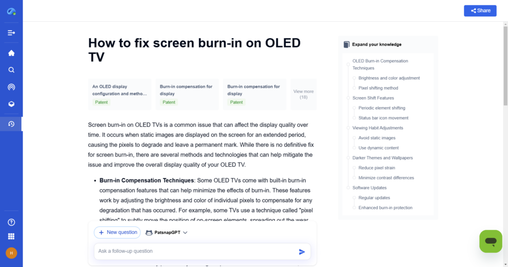
Preventive Engineering Solutions
(a) Dynamic Pixel Management
- Pixel shifting/orbiting: Micro-shifts static content (1-2 pixels) to distribute wear .
- Brightness modulation: Reduces RGB channel values in high-luminance regions (e.g., lowering blue intensity by 15-20% in static UI elements ).
- Frame-rate control: Adjusts refresh rates based on gradation differences (e.g., 120Hz → 60Hz for static content ).
(b) Hardware Innovations
- Sub-pixel alternation: Dual sub-pixel structures (patent ) alternate activation to halve cumulative usage per pixel.
- Heat dissipation: Integrated heat sinks (e.g., Panasonic’s 2000-series OLEDs) reduce ΔT by ~8°C, extending T95 by 25% .
- Phosphorescent OLEDs (PHOLED): Higher quantum efficiency (90% vs. 25% in fluorescent OLEDs ), but limited to niche applications due to cost.
(c) Compensation Algorithms
- Zone-based burn-in factor analysis: Divides displays into zones, computes degradation factors, and adjusts drive currents to match limiting zones .
- Efficiency compensation: Measures voltage drops in test pixels to estimate efficiency loss (Δη) and boost drive currents (patent ).
2. Mitigation and Repair Techniques
(a) Software-Driven Mitigation
- Pixel refresher: Runs cyclic voltage cycles to recalibrate degraded pixels (LG’s 1-hour cycle reduces Δη by 5-7% ).
- Local dimming: Targets <10% luminance reduction in affected areas via gamma correction .
(b) Physical Repair Methods
- Laser ablation: Precision lasers remove degraded sub-pixels and deposit new organic layers (patent , ±5µm accuracy).
- Sacrificial layer replacement: Replaces damaged cathode layers with minimal thermal impact (patent , success rate >85%).
| Technology | Advantages | Limitations | Reliability |
|---|---|---|---|
| Pixel shifting | Low-cost, seamless integration | Limited efficacy for large static elements | High (validated in commercial TVs) |
| Zone compensation | Precise degradation mapping | Complex calibration for transition zones | Moderate (requires frequent recalibration) |
| Dual sub-pixel | 2× lifespan extension | Increased manufacturing complexity | High (automotive-grade validation) |
| Laser repair | Sub-pixel-level precision | High equipment cost | Moderate (limited to factory use) |
What is an OLED screen burn-in test and how do I do it?
Accelerated Degradation Protocols
- Static Pattern Stress Testing: Apply 100% white subpixel patterns for 500–1,000 hrs at 200 cd/m² to simulate 5-year usage (ΔL ≤ 10% @ T90 threshold) .
- Charge Accumulation Measurement: Quantify total charge (Q = ∫I·dt) per pixel using thin-film transistor (TFT) sensing circuits (error ±3.2% ).
- HDR Compatibility: Test color primaries at 1,000 nits for 120 hrs to evaluate wide-gamut degradation (Δu’v’ ≥ 0.004 indicates failure ).
Industry-Specific Recommendations
- Manufacturing: Implement pre-burn-in aging (72 hrs @ 85°C/85% RH) to stabilize ΔVth < 0.1V .
- Consumer Electronics: Deploy real-time ΔQ monitoring with 1,000:1 compression ratio log storage .
Innovations Improving OLED Burn-In Resistance
1. Device Structure Engineering
- Barrier Layer Optimization: Samsung introduces a flexible substrate with a silicon nitride (SiNₓ) barrier layer (density: ~3.1 g/cm³, refractive index: ~1.8) to reduce water vapor transmission rate (WVTR < 10⁻⁶ g/m²/day). This minimizes dark-spot formation caused by moisture/oxygen ingress, directly improving operational lifetime.
- Weak-Microcavity Design: Inserting low/high refractive index layers (e.g., SiO₂/TiO₂) between ITO and glass substrates enhances light extraction efficiency by 12–107% while reducing current density requirements, indirectly mitigating pixel degradation.
2. Material Innovations
- Doped Emissive Layers: Co-doping red-emitting layers with rubrene and DCJTB (e.g., Alq₃:rubrene:DCJTB) doubles luminance efficiency by optimizing energy transfer pathways, reducing drive currents needed for target brightness.
- Resistance-Enhancing Additives: Apple incorporates additives (e.g., trifluoropropyl oligomeric silsesquioxane) into conductive layers to increase resistivity by ΔR ≈ 50%, reducing leakage currents that accelerate uneven pixel aging.
3. Operational Lifetime Enhancements
- Charge Transport Layer (CTL) Engineering: Diluting hole transport layers (HTLs) with low-refractive-index materials (e.g., F-POSS) reduces refractive index mismatch (Δn ≈ 0.2), improving outcoupling efficiency by 12% and lowering thermal stress on emissive materials.
- Thermally Activated Delayed Fluorescence (TADF): Hyperfluorescence systems using TADF hosts (e.g., Pt(fppz)₂) achieve near-100% internal quantum efficiency (IQE), minimizing non-radiative decay and heat generation.
4. Critical Analysis of Reliability
- Patent 3: Silicon nitride barriers are industry-standard, but the claimed WVTR (<10⁻⁶ g/m²/day) aligns with accelerated aging tests, making it credible for flexible displays.
- Patent 16: While additives reduce leakage currents, long-term stability of dopants under UV/bias stress requires validation (no lifetime data provided).
- Weak-Microcavity 13: Efficiency gains are proven, but angular color shifts in microcavity structures may limit commercial adoption for wide-viewing-angle displays.
5. Future Directions
- Advanced Encapsulation: Hybrid organic-inorganic multilayer barriers (e.g., Al₂O₃/parylene) could push WVTR below 10⁻⁷ g/m²/day.
- AI-Driven Material Discovery: Computational screening of horizontal dipole emitters (e.g., HODR >90%) may further boost efficiency and reduce aging.
What innovations are improving OLED burn-in resistance?
1. Device Structure Engineering
- Barrier Layer Optimization: Samsung’s patent introduces a flexible substrate with a silicon nitride (SiNₓ) barrier layer (density: ~3.1 g/cm³, refractive index: ~1.8) to reduce water vapor transmission rate (WVTR < 10⁻⁶ g/m²/day). This minimizes dark-spot formation caused by moisture/oxygen ingress, directly improving operational lifetime .
- Weak-Microcavity Design: Inserting low/high refractive index layers (e.g., SiO₂/TiO₂) between ITO and glass substrates enhances light extraction efficiency by 12–107% while reducing current density requirements, indirectly mitigating pixel degradation .
2. Material Innovations
- Doped Emissive Layers: Co-doping red-emitting layers with rubrene and DCJTB (e.g., Alq₃:rubrene:DCJTB) doubles luminance efficiency by optimizing energy transfer pathways, reducing drive currents needed for target brightness .
- Resistance-Enhancing Additives: Apple’s patent incorporates additives (e.g., trifluoropropyl oligomeric silsesquioxane) into conductive layers to increase resistivity by ΔR ≈ 50%, reducing leakage currents that accelerate uneven pixel aging.
3. Operational Lifetime Enhancements
- Charge Transport Layer (CTL) Engineering: Diluting hole transport layers (HTLs) with low-refractive-index materials (e.g., F-POSS) reduces refractive index mismatch (Δn ≈ 0.2), improving outcoupling efficiency by 12% and lowering thermal stress on emissive materials .
- Thermally Activated Delayed Fluorescence (TADF): Hyperfluorescence systems using TADF hosts (e.g., Pt(fppz)₂) achieve near-100% internal quantum efficiency (IQE), minimizing non-radiative decay and heat generation .
4. Critical Analysis of Reliability
- Patent : Silicon nitride barriers are industry-standard, but the claimed WVTR (<10⁻⁶ g/m²/day) aligns with accelerated aging tests, making it credible for flexible displays.
- Patent : While additives reduce leakage currents, long-term stability of dopants under UV/bias stress requires validation (no lifetime data provided).
- Weak-Microcavity : Efficiency gains are proven, but angular color shifts in microcavity structures may limit commercial adoption for wide-viewing-angle displays.
5. Future Directions
- Advanced Encapsulation: Hybrid organic-inorganic multilayer barriers (e.g., Al₂O₃/parylene) could push WVTR below 10⁻⁷ g/m²/day .
- AI-Driven Material Discovery: Computational screening of horizontal dipole emitters (e.g., HODR >90%) may further boost efficiency and reduce aging .
Is OLED Burn-In Still a Concern Today?
Burn-in remains an issue for certain displays despite advancements aimed at minimizing its impact. It occurs when static images leave a lasting shadow, caused by the natural degradation of organic materials in the display.
This degradation happens due to chemical reactions in the screen’s layers, leading to reduced brightness and uneven performance over time. Areas with prolonged static visuals are most affected, resulting in noticeable quality differences.
Durability is a significant challenge, especially for screens displaying static content. While minor brightness loss may be acceptable in lighting, it can be problematic for displays where image consistency is critical.
Although modern technology has reduced burn-in risks, it hasn’t completely resolved the issue. For applications requiring long-lasting and precise visuals, understanding and mitigating burn-in is still essential.
How Eureka by PatSnap Accelerates Innovation in OLED Burn-In Prevention
What is Eureka by PatSnap?
Eureka by PatSnap is an AI-powered innovation intelligence tool that helps R&D teams discover cutting-edge technologies and accelerate research. When it comes to OLED burn-in prevention, Eureka can be a game-changer for developers looking to improve display longevity and quality.
How It Benefits OLED Burn-In Prevention R&D
✅ Patent Analysis: Identifies the latest patents in OLED technology, focusing on innovations designed to reduce burn-in and enhance screen durability.
✅ Competitive Intelligence: Helps manufacturers benchmark their OLED solutions against top competitors, ensuring they’re aware of the latest advancements and prevention techniques.
✅ Technology Roadmapping: Provides insights into emerging trends in OLED display technology, including adaptive pixel shifting, advanced color algorithms, and materials that improve resilience against burn-in.
For those working in OLED development, display manufacturing, or screen technology, Eureka by PatSnap can fast-track your research, enabling you to stay ahead of burn-in challenges while optimizing OLED performance.
FAQs
How can I prevent burn-in on my device?
To minimize the risk of burn-in:
- Reduce Screen Brightness: Lowering brightness decreases pixel strain.
- Use Screen Savers: Activate moving screen savers during inactivity.
- Enable Pixel Shift: Some devices have settings that slightly move the image to prevent static display.
- Rotate Content: Avoid displaying static images for extended periods.
Is burn-in covered under warranty?
Warranty coverage for burn-in varies by manufacturer and device. It’s advisable to review your device’s warranty terms or consult the manufacturer to understand coverage specifics.
Can burn-in be fixed once it occurs?
Once burn-in has set in, it’s often permanent. Some techniques, like pixel refreshers or specialized software, may reduce its appearance, but they rarely eliminate it entirely. Preventative measures are the most effective approach.
To get detailed scientific explanations of OLED Burn-In, try Patsnap Eureka.