Applied Materials, Inc., headquartered in Santa Clara, California, is the world’s largest supplier of equipment, services, and software for manufacturing semiconductors and displays. With a technology portfolio that touches nearly every chip on Earth, the company is enabling the next generation of computing, from AI and high-performance computing (HPC) to 5G and edge devices.
This article explores Applied Materials’ corporate blueprint, engineering breakthroughs, global footprint, and financial health. With PatSnap Eureka AI Agent, we uncover Applied’s IP architecture, technological evolution, and competitive edge in atomic-scale materials control and semiconductor system integration.
Ask Patsnap Eureka AI
Patsnap Eureka AI provides instant, trusted answers to any technical questions.
OLED, QLED, LCD, rollable and foldable display solutions
Corporate Ventures
Strategic investments in frontier technologies (quantum computing, photonics, AI)
Office of the CTO
Long-term R&D, ecosystem collaborations, university partnerships
Each unit operates synergistically, allowing Applied to offer end-to-end process innovation, enhancing fab productivity and yield.
Business Model and Services
Applied Materials operates a high-touch B2B model integrated into the supply chains of the world’s top semiconductor and display companies. Key components:
Capital Equipment Sales: Wafer processing systems that enable transistor formation, interconnect, and packaging.
Process Development: Customization of fabrication steps to meet unique customer node requirements (e.g., Gate-All-Around FET, 3D NAND).
Service & Upgrades: Installed base optimization through software enhancements, automation, and analytics (via Applied Global Services).
AI-Integrated Systems: Platforms like AIx™ use real-time machine learning to adjust process variables dynamically.
Innovation & Technology
Applied Materials leads the semiconductor industry through an unmatched portfolio of tools and platforms that control materials at atomic precision. Its innovation strategy revolves around the Materials to Systems™ paradigm, which focuses on controlling the interactions between substrates, plasma, and process chambers to meet the complex requirements of next-generation semiconductor devices.
At the heart of Applied’s systems are its semiconductor processing chambers, engineered to provide precise control over:
Plasma uniformity
Substrate temperature and support mechanics
Reactive gas flow distribution
Deposition and etch chemistry
Each reaction chamber is optimized for specific processes like CVD, PVD, ALD, or plasma etch. Substrate handling innovations, such as electrostatic chucks and heat transfer interfaces, ensure nanometer-level control of film thickness and stress profiles.
Common technologies integrated into chambers include:
Plasma sources with RF/microwave excitation
Process monitoring sensors for in-situ metrology
Multi-zone substrate heating modules
These chamber-centric innovations are central to Applied’s IP portfolio. According to PatSnap Eureka AI Agent, top patent clusters include “semiconductor processing chamber,” “substrate support,” and “plasma processing unit,” reflecting the company’s sustained leadership in process architecture.
2. AI-Driven Process Optimization (AIx Platform)
Applied’s AIx™ system integrates machine learning and edge computing directly into tools—particularly those used for substrate processing and etch uniformity control. AIx can detect anomalies in plasma stability, deposition rate drift, or substrate alignment, and adjust process parameters in real-time.
Use case: In a complex chemical mechanical polishing (CMP) process, AIx detects pad wear and dynamically alters pressure zones to maintain wafer planarity across batches.
3. Integrated Materials Solutions (IMS)
IMS is Applied’s strategy to combine multiple substrate processing steps—like pre-clean, film deposition, and annealing—within a single vacuum-sealed cluster.
Key benefits include:
Reduced substrate exposure time between steps
Elimination of particle contamination
Higher yield and throughput per process chamber
A typical IMS cluster might integrate:
A deposition chamber (e.g., for low-k film)
A plasma processing module (e.g., for densification)
A substrate cooling/heating station with real-time metrology
4. Deposition & Surface Engineering Technologies
Applied’s deposition technologies support the fabrication of highly scaled devices like 3D NAND, FinFET, and GAA transistors. Its systems deliver unmatched precision for:
Deposition Type
Application
CVD / PECVD
Gate dielectrics, spacers, isolation layers
PVD (Endura®)
Metallization of interconnects, barrier/liner formation
Key features of Applied’s deposition process IP include:
Multi-zone gas injection for uniform film growth
Real-time plasma source modulation
Reactive species control for tunable stoichiometry
5. Patterning & Post-Litho Integration
With shrinking nodes, Applied focuses heavily on patterning fidelity enhancement. It offers etch and clean systems that enable:
Selective etch with atomic-layer precision
Aspect-ratio independent etching for deep features
Post-lithography plasma treatments to reduce line edge roughness
Its etching platforms are deeply integrated with metrology and substrate rotation stages to ensure uniform plasma exposure.
6. System-Level Process Control and Interoperability
Applied emphasizes tool-to-tool connectivity, where process chamber modules, substrate handling arms, and diagnostic sensors exchange data in real-time. This modular interoperability enables:
Cross-platform process co-optimization
Fast recipe tuning across multiple chambers
Inline defectivity management via AI feedback
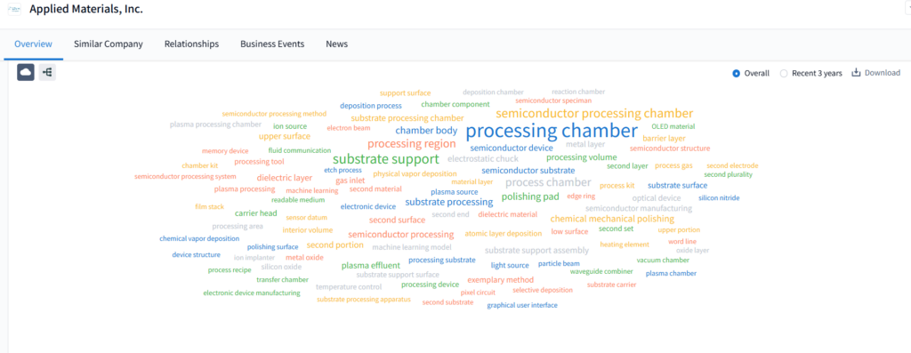
PatSnap Eureka AI Agent Capabilities
PatSnap Eureka AI Agent enables in-depth exploration of Applied’s process chamber and substrate-centric innovations through:
Patent Word Cloud Analysis: High-frequency terms like processing chamber, substrate support, plasma source, chemical mechanical polishing, and reaction chamber dominate Applied’s recent filings.
Time-Filtered Innovation Matrix: Visualizes how focus shifted from simple PVD chambers (2010–2015) to AI-enhanced plasma control and substrate feedback systems (2020–2024).
Semantic Clustering: Groups patents related to “semiconductor substrate temperature regulation,” “etch endpoint detection,” and “vacuum chamber integration,” revealing Applied’s full-stack control approach.
Market Presence and Financials
Metric
Details
Global Reach
Offices in >90 countries
Manufacturing Facilities
U.S., Israel, Singapore, Taiwan
R&D Investment (2024)
~$3.2 Billion (~12% of Revenue)
Top Growth Markets
Taiwan, South Korea, China, Japan, USA
Revenue Breakdown
70% Semiconductor Systems, 20% Global Services, 10% Display
Applied’s customer stickiness is driven by co-development partnerships and long-term service contracts. In the AI era, growth is fueled by rising wafer starts and new packaging demand.
Competitive Landscape
Company
Specialization
Differentiator
ASML
EUV Lithography
Monopoly on EUV systems
Lam Research
Etch and Clean
Precision etch at advanced nodes
Tokyo Electron
Coater/Developer, Etch, Deposition
Strong in Japan & Korea; collaborative with TSMC
Applied Materials
Deposition, Etch, Metrology, AIx™
Integrated material-to-system solutions + AI/ML
With ~15,000 active patents, Applied leads in patent volume and cross-node adaptability, a position verified by PatSnap Eureka’s Competitor Benchmarking Dashboard.
ESG & Sustainability
Applied is committed to reducing carbon intensity per wafer pass by 50% by 2030 and building low-GWP process gases and energy-efficient tools. Highlights include:
EPIC R&D Center: A $4B initiative to accelerate sustainable semiconductor design.
Supplier Sustainability Scorecard: Enforces ESG targets across its global supply chain.
Diversity & Inclusion: “Opportunity Knocks” program launched to upskill underserved communities.
Conclusion
Applied Materials exemplifies how relentless innovation, vertical integration, and deep customer partnerships can deliver scalable value in the age of AI and quantum computing. By investing in sustainable technologies and smart manufacturing, it is not only powering the chips of tomorrow but also reshaping the future of materials science.
Through PatSnap Eureka’s Company Search AI Agent, we can decode how Applied’s patents, platform evolution, and competitive moves align with industry megatrends—equipping businesses, researchers, and investors with the intelligence needed to stay ahead.